


Paper Sharing
【International Papers】Researchers from the University of California San Diego of Low-temperature pressure-assisted liquid-metal printing for β-Ga₂O₃ thin-film transistors
日期:2025-02-25阅读:1047
Researchers from the University of California San Diego have published a dissertation titled "Low-temperature pressure-assisted liquid-metal printing for β-Ga2O3 thin-film transistors" in Nature Communications.
Author Introduction

Nomura's research is interdisciplinary and spans the fields of material science and device physics. His expertise lies in the development of wide bandgap semiconductor and electronic devices. His research opens the field of amorphous oxide semiconductor based thin-film transistor technology and significantly contributes to the advancement of oxide electronics. One key objective of his current research is to develop new amorphous oxide semiconductor materials and high-performance electronic devices for next generation wearable electronics, such as display and sensor applications. His group also has interest in advanced oxide-based nanostructured electronic devices. His research group works on a variety of aspects from material design, syntheses, film growth to device modeling, fabrication and testing based on theoretical and experimental approaches. His research aims to further develop oxide semiconductor device technology based on novel material development.
Abstract
Developing a low-temperature and cost-effective manufacturing process for energy-efficient and high-performance oxide-thin-film transistors (TFTs) is a crucial step toward advancing next-generation device applications such as wearable and flexible electronics. Among several methods, a liquid-metal printing technique is considered a promising, cost-effective oxide semiconductor process due to its inherent advantages, such as vacuum-free, low-thermal budget, high throughput, and scalability. In this study, we have developed a pressure-assisted liquid-metal printing technique enabling the low-temperature synthesis of polycrystalline wide bandgap n-channel oxide-TFTs. The n-channel oxide TFTs based on ~3 nm-thick β-Ga2O3 channels exhibited good TFT switching properties with a threshold voltage of ~3.8 V, a saturation mobility of ~11.7 cm2 V−1 s−1, an on/off-current ratio of ~109, and a subthreshold slope of ~163 mV/decade. We also observed p-channel operation in the off-stoichiometric GaOx channels fabricated at high-pressure conditions. Toward oxide-based circuit applications, we developed high-performance oxide-TFT-based inverters. While our approach can promote the advancement of low-temperature manufacturing for oxide TFT technology, further work will be necessary to confirm the role of the applied pressure in the β-Ga2O3 crystallization process.
Experimental Diagram
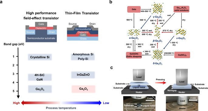
Fig. 1: Pressure-assisted liquid-metal printing for β-Ga2O3 thin-film transistors (TFTs). a Motivation and purpose for developing low-temperature processed wide-bandgap Ga2O3 TFTs. b Phase transformation relationship for Ga2O3 polymorphism. c Schematic and photographs of the developed pressure-assisted liquid metal printing routes for Ga2O3 nanosheet fabrication.
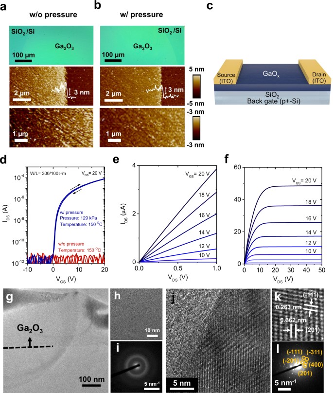
Fig. 2: Material and electrical characterization of Ga2O3 films. Optical microscopy image and atomic force microscopy (AFM) image (including cross-sectional step-height profile) for the Ga2O3 nanosheet were prepared by a conventional liquid metal printing (LMP) (without applied printing process pressure) and b pressure-assisted liquid metal printing (PA-LMP) methods (applied printing process temperatures (Tp) of 150 °C and printing process pressure (Pp) of 129 kPa). c Schematics of the device structure of the GaOx thin-film transistors (TFTs). d Typical transfer characteristics for the Ga2O3 TFTs prepared by LMP (Tp of 150 °C and Pp of 0 kgf/cm2)) and PA-LMP (Tp of 150 °C and Pp of 129 kPa) methods. (IDS: drain currents, VDS: drain-to-source voltage, VGS: gate bias) The channel width (W) and length (L) of TFTs are 300 and 100 µm, respectively. e Magnified view of the linear regime in the typical output characteristics for the Ga2O3 TFT. f Typical output characteristics for the Ga2O3 TFT. g Low-magnified high-resolution transmission electron microscopy (HRTEM) images of the Ga2O3 nanosheet synthesized by the conventional LMP route. (without applied printing process pressure) Corresponding h high-magnified HRTEM image and i selected area electron diffraction (SAED) pattern. j Low-magnified HRTEM images of Ga2O3 nanosheet synthesized by the pressure-assisted liquid-metal route. (Tp of 150 °C and Pp of 129 kPa) Corresponding k high-magnified HRTEM image and l SAED pattern.
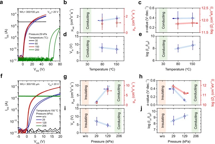
Fig. 3: Effect of the printing process on Ga2O3 thin-film transistor (TFT) performance.a Variation of transfer characteristics for the Ga2O3 nanosheet TFTs with different printing process temperatures under the uniaxial process pressure of 29 kPa. The corresponding TFT parameters b saturation mobility (μsat) and linear mobility (μlin), c subthreshold swing (s-value) and trap-state density (Dit), d threshold voltage (Vth), and e on/off current ratio are plotted. f Variation of transfer characteristics for the Ga2O3 TFTs with different process pressures under the printing process temperature of 150 °C. Corresponding TFT parameters g μsat and μlin, h s-value and Dit, i Vth, and j on/off current ratio are plotted. (The error bars are calculated using data from 16 representative working devices across different samples).
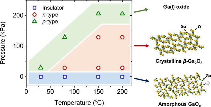
Fig. 4: Electrical properties of Ga2O3 films grown by liquid-metal printing. Summary of the electrical properties of the gallium oxide nanosheet channel grown using the pressure-assisted liquid-metal route under various printing process conditions of uniaxial pressures and temperatures.
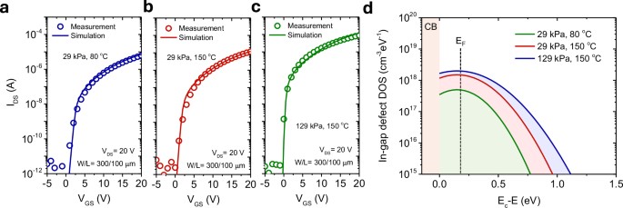
Fig. 5: TCAD simulation of Ga2O3 thin-film transistors (TFTs).
Comparison of measured (symbols) and simulated (lines) transfer curves with VDS = 20 V for the Ga2O3 TFTs with different printing process conditions. (a Tp of 80 °C, Pp of 29 kPa, b Tp of 150 °C, Pp of 29 kPa, c Tp of 150 °C, Pp of 129 kPa). d Corresponding in-gap density of states (DOS) profiles for the Ga2O3 nanosheet channels for different printing process conditions. Fermi level (EF) lies at Ec − EF = 0.23 eV. (Ec: conduction band edge energy, CB:conduction band.) TCAD simulations were conducted to extract the in-gap defect DOS profile in Ga2O3 TFTs. The measured I-V curves were accurately modeled by optimizing only the acceptor-like defects (electron trap states) using a Gaussian distribution, gG(E) = NGD × exp[-(Ec-EGA)^2 / (2×WGD^2)], where NGD is the state densities at the central energy EGA of the Gaussian distribution, Ec is the conduction band edge energy for the reference zero point, EGA is the central energy of gG(E), WGD is the characteristic decay energy.
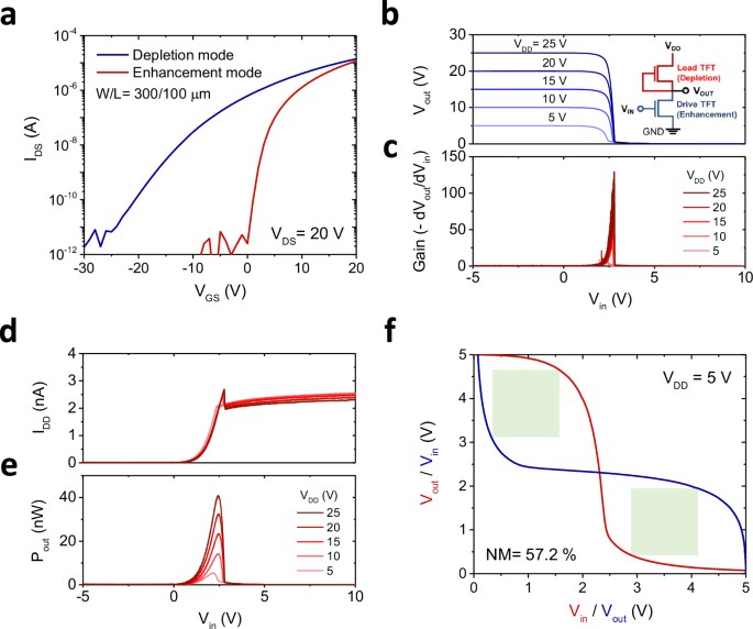
Fig. 6: Ga2O3 transistor-based N-channel Metal-Oxide-Semiconductor (NMOS) inverter. An NMOS inverter is a logic circuit built using an n-channel MOSFET (NMOS transistor) and a pull-up resistor or load transistor. a Typical transfer characteristics for the depletion-mode and enhancement-mode Ga2O3 TFTs. (The Ga2O3 nanosheets used for the NMOS circuits demonstration were grown using the Tp of 150 °C, Pp of 29 kPa. The depletion-mode TFTs were fabricated by performing post-thermal annealing under vacuum conditions at 100 °C.) b Voltage transfer characteristic (VTC) of the Ga2O3 TFT-based NMOS inverter. c corresponding voltage gains of the Ga2O3 TFT-based NMOS inverter. Inset: schematic circuit diagram of the zero-VGS-load NMOS inverter composed of enhancement/depletion-mode Ga2O3 TFTs. d Corresponding supply currents (IDD). e Output-power consumption (Pout) for the Ga2O3 TFT-based NMOS inverter. f Butterfly curves for noise margin (NM) of the Ga2O3 TFT-based NMOS inverter. (Vin: input voltage, Vout: output voltage, VDD: supply voltage).
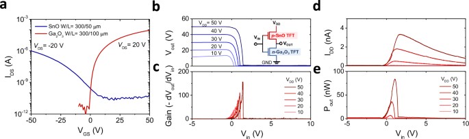
Fig. 7: N-Ga2O3/p-SnO transistor-based complementary metal-oxide-semiconductor (CMOS) inverter. A CMOS inverter is a logic circuit consisting of a p-channel MOSFET (PMOS) as the pull-up device and an n-channel MOSFET (NMOS) as the pull-down device. a Typical transfer characteristics of the ultrathin p-channel SnO TFT with VDS = −20 V and n-channel Ga2O3 TFTs at VDS = 20 V. (The Ga2O3 nanosheets used for the CMOS circuits demonstration were grown using the Tp of 150 °C, Pp of 29 kPa.) b Voltage transfer characteristics (VTC). c Corresponding voltage gains for the p-SnO/n-Ga2O3 TFT-based CMOS inverter. Inset: schematic of the corresponding oxide-TFT-based CMOS inverter circuit. d Corresponding supply currents (IDD). e Output-power consumption (Pout) for p-SnO/n-Ga2O3 TFT-based CMOS inverter.
DOI:
doi.org/10.1038/s41467-025-57200-2
