Paper Sharing
【Member Papers】Xidian University - Chang Jingjing, Lin Zhenhua, Gao Xiangxiang AELM: Photo-Synaptic Memristor Devices from Solution-Processed Ga₂O₃ Thin Films
日期:2025-02-27阅读:852

A research paper titled "Photo-synaptic Memristor Devices from Solution-processed Ga2O3 Thin Films" was reported by Chang Jingjing research group of Xidian University. In this study, photosynaptic devices based on Ga2O3 resistive memory are prepared by solution processed. By optimizing the solution concentration and annealing temperature, non-volatile memory is realized. The switching ratio of the device is greater than 104, and the stable holding time of the resistive state is more than 104 s, which has a high memory life. At the same time, the synaptic behaviors such as excitatory postsynaptic current and double pulse facilitation are observed by using ultraviolet signal as stimulus signal, which proves the feasibility of realizing simulated synapses. Finally, by simulating a series of learning-forgetting processes, the device has great application potential in the field of neuromorphic vision.
Research Background
The human brain has a highly developed sensory-memory-computing capacity, and the transmission and processing of information in the human brain is done through a large number of neurons and synapses. As an important connection between neurons, synapses have the function of simultaneously storing and processing information, which endows neurons with remarkable computing power. Therefore, designing physical devices with synaptic behavior is a critical step in building brain-like computing. Resistive random access memory (RRAM) is an important candidate for mimicking the function of biological synapses because it has a structure similar to that of biological synapses and can scale down the device size so that the device can reach an order of magnitude of the density of synapses in the human brain.
Graphic Interpretation

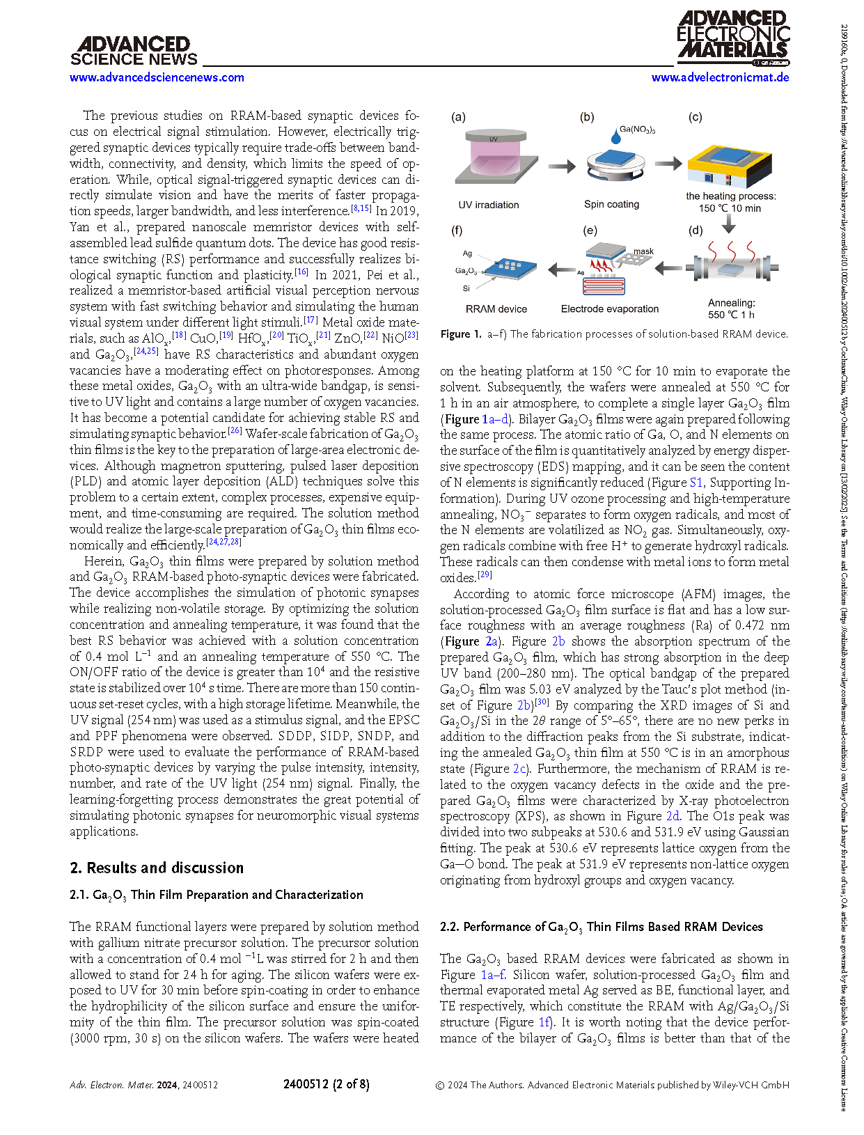
Figure 1. a-f) The fabrication processes of solution-based RRAM device.

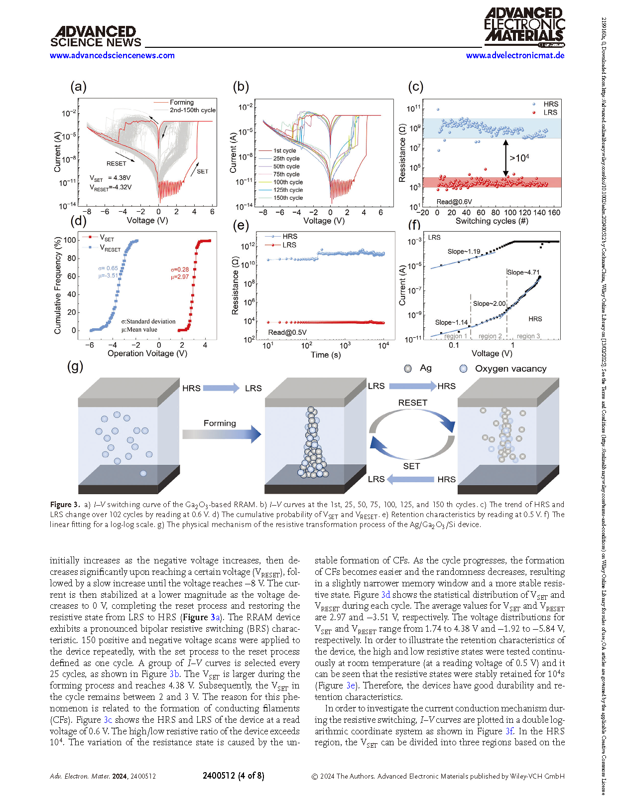
Figure 2. I–V switching curve of the Ga2O3-based RRAM. b) I–V curves at the 1st, 25, 50, 75, 100, 125, and 150 th cycles. c) The trend of HRS and
LRS change over 102 cycles by reading at 0.6 V. d) The cumulative probability of VSET and VRESET. e) Retention characteristics by reading at 0.5 V. f) The
linear fitting for a log-log scale. g) The physical mechanism of the resistive transformation process of the Ag/Ga2O3/Si device.
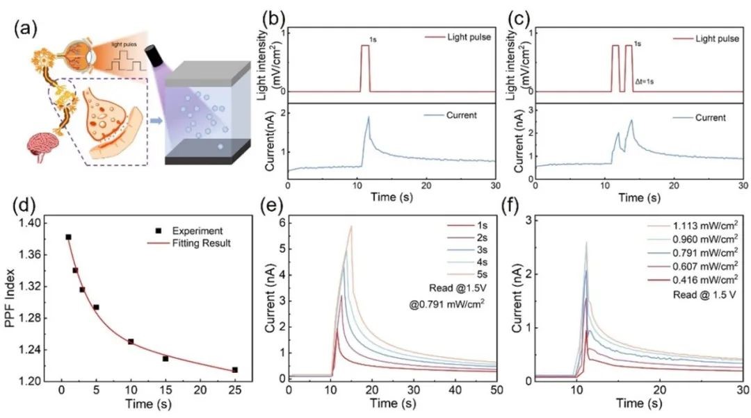
Figure 3. a) Schematic diagram of the human visual system and RRAM-based photonic synapse structure. Synaptic EPSC b) and PPF c) functions are
triggered by a single UV pulse (0.791 mW cm−2, 1 s) and a pair of pulses (Δt = 1 s), respectively. d) Fitting the relationship of PPF index with pulse
interval Δt using a double exponential fitting. The currents under a single UV peak with varied light duratione) and light intensityf).

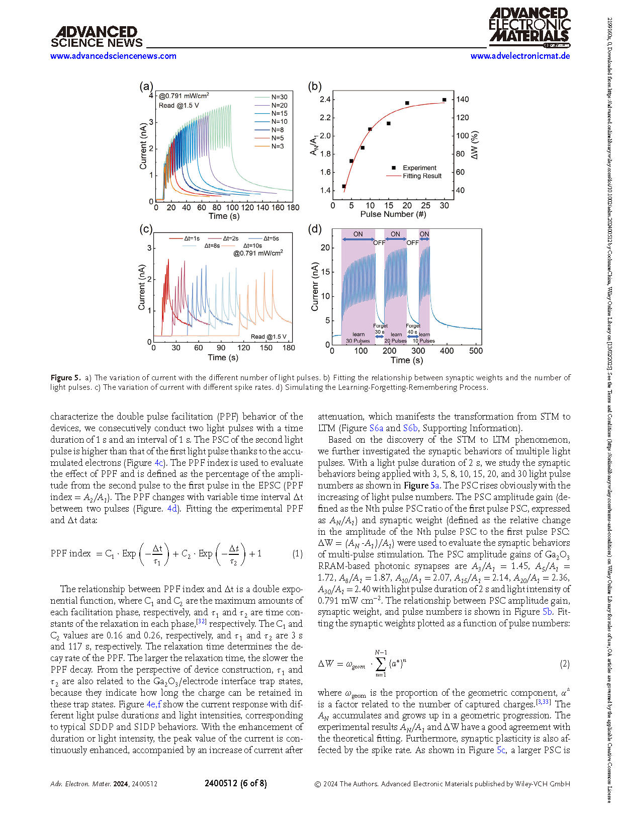
Figure 4. a) The variation of current with the different number of light pulses. b) Fitting the relationship between synaptic weights and the number of
light pulses. c) The variation of current with different spike rates. d) Simulating the Learning-Forgetting-Remembering Process.
The optical synaptic device based on solution processed proposed by the team has excellent memory performance such as high impedance state stable holding time and high switching ratio. In addition, when stimulated by ultraviolet light (254 nm), the device achieves synaptic plasticity and can be used to simulate biological synapses. Finally, through the learn-forget-memory simulation, the Ga2O3 RRAM-based optical synaptic device is verified to have the ability of information storage, revealing the great potential of RRAM-based optical synapses in brain memory.
Original Link:
https://onlinelibrary.wiley.com/doi/10.1002/aelm.202400512