Paper Sharing
【Domestic Papers】Researchers Led by Academician Deren Yang from the Zhejiang University——Characterization of dislocations in (-310) β-Ga₂O₃ single crystal grown by the casting method
日期:2025-02-27阅读:997
Researchers from the Zhejiang University have published a dissertation titled "Characterization of dislocations in (-310) β-Ga2O3 single crystal grown by the casting method" in Journal of Alloys and Compounds.
Program Support
This work was supported by the (Pioneer) and (Leading Goose) R&D Program of Zhejiang (2023C01193), the National Natural Science Foundation of China (52202150, 22205203, and 62204218), Fundamental Research Funds for the Central Universities (226-2022-00200 and 226-2022-00250), the National Postdoctoral Program for Innovative Talents (BX20220264), the National Program for Support of Topnotch Young Professionals, and the Leading Innovative and Entrepreneur Team Introduction Program of Hangzhou (TD2022012).
Background
β-Ga2O3 is a newly prominent ultra-wide bandgap semiconductor material with significant potential for applications in optoelectronic and power electronic devices. However, the presence of dislocations in the single crystal poses severe challenge to the performance and reliability of devices, thus, needed to be minimized. Recent studies have shown that the (-310) plane of β-Ga2O3 holds promise as a close-packed plane for epitaxial growth and devices fabrication.
Abstract
The (-310)-oriented β-Ga2O3 substrate serves as a promising close-packed plane for epitaxial growth and devices fabrication. Dislocations, which are major crystal defects in β-Ga2O3, negatively impact the performance and reliability of electronic devices. In this paper, we investigated dislocations on the (-310) plane by X-ray topography, transmission electron microscopy, chemical etching and atomic force microscopy. Our findings confirm the formation of mixed dislocation loops generated during simultaneously nucleation in the crystal growth process via the casting method. These loops are primarily composed of screw-type dislocations with a Burgers vector b = <010 > on the {001} slip plane and the corresponding etch pits delineated by H3PO4 solution are water droplet like arrays along [130] orientation on the (-310) plane. DFT calculations revealed the < 010 > / {001} was the easiest slip system in β-Ga2O3 and the crystallographic features of the water droplet like pit were thoroughly explained. This comprehensive analysis offers valuable insights for optimizing processing techniques to reduce dislocations and enhance material quality for device applications.
Highlights
· The study pioneers the growth and fabrication of the (-310) β-Ga2O3substrates using the casting method, offering a novel plane for homoepitaxial and heteroepitaxial growth.
· Through advanced techniques such as X-ray topography, TEM, and preferential etching, the article identifies mixed dislocation loops dominated by screw-type dislocations with a Burgers vector b = <010 > beneath the water droplet etch pits, providing the first in-depth characterization of defects on the (-310) plane.
· The findings provide critical insights into reducing dislocations, paving the way for improved substrate quality and enhanced performance in power device applications.
Graphic abstract
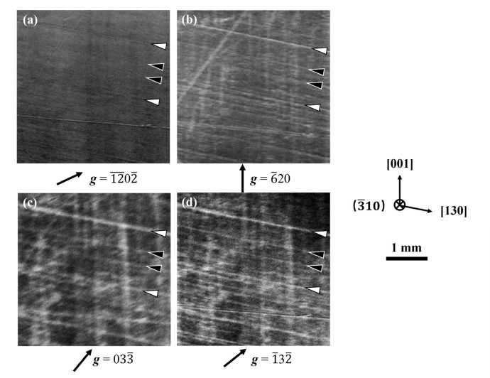
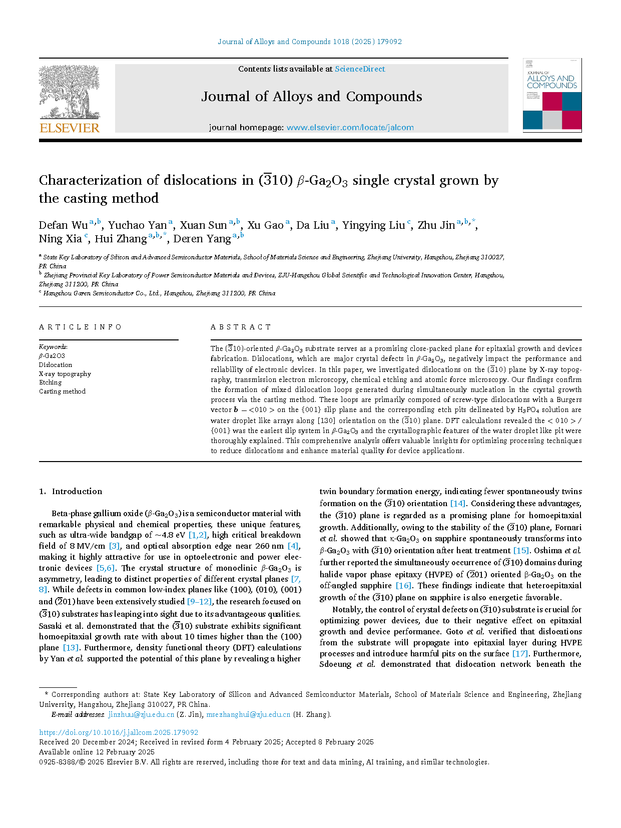
Fig. 1. XRT images captured at (a) g = -1-202, (b) g = -620, (c) g = 03-3 and (d) g = -13-2, respectively.
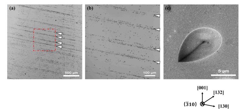
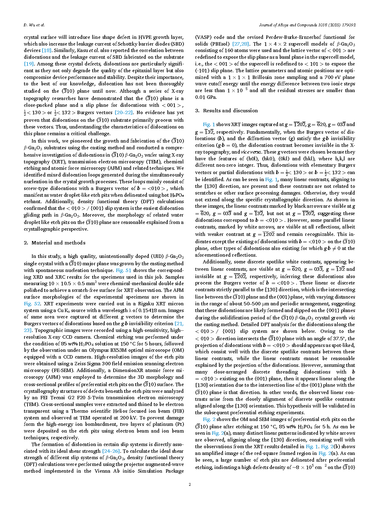
Fig. 2. (a-b) OM image and (c) FE-SEM image of etch pits on the (-310) plane etched at 150°C 85 wt% H3PO4 for 5 h.
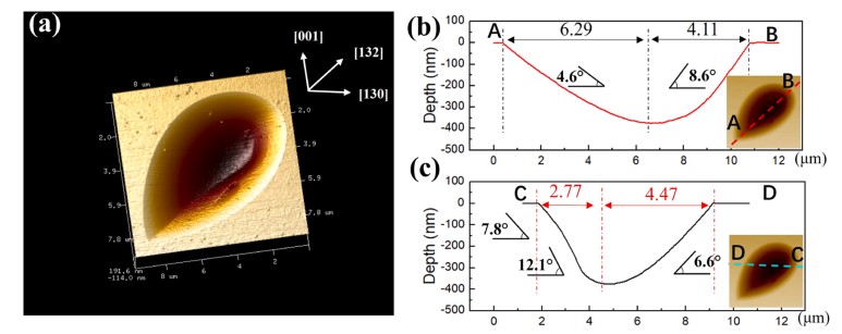
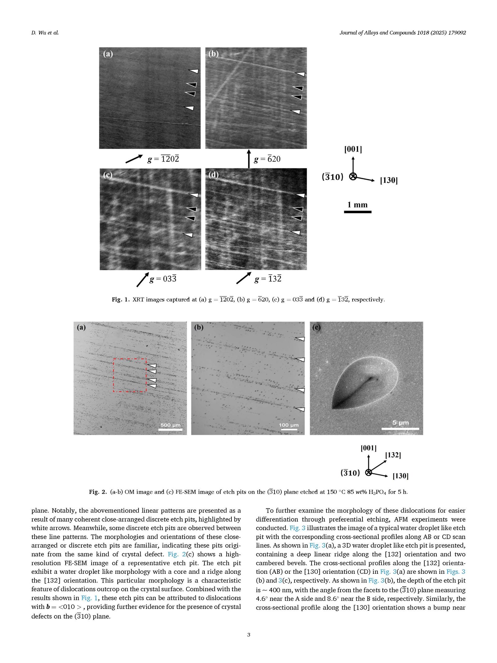
Fig. 3. (a) AFM image of a water droplet like pit, cross-sectional profiles alone (b) AB or (c) CD scan lines.
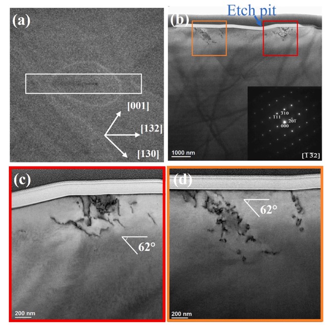
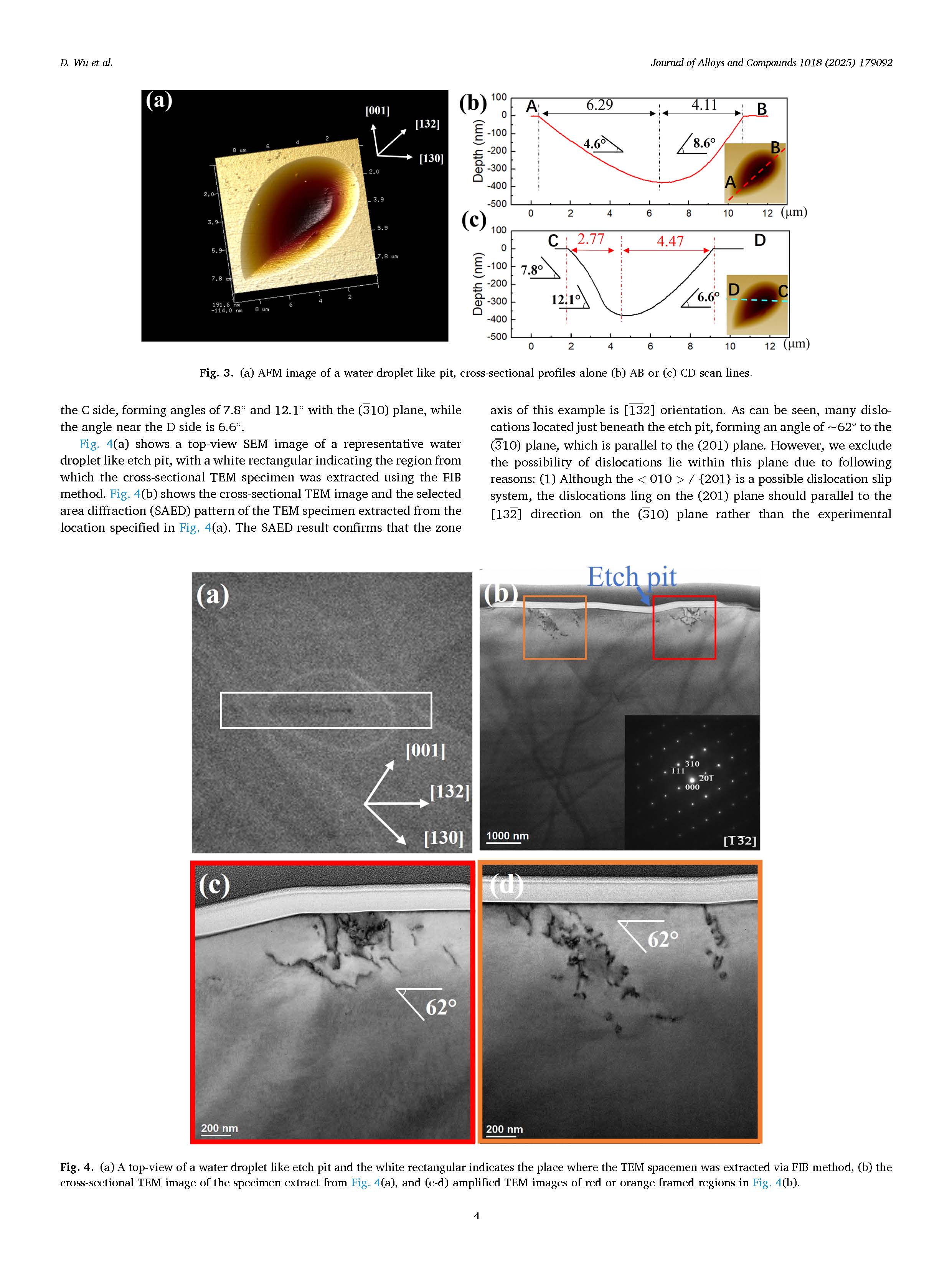
Fig. 4. (a) A top-view of a water droplet like etch pit and the white rectangular indicates the place where the TEM spacemen was extracted via FIB method, (b) the cross-sectional TEM image of the specimen extract from Fig. 4(a), and (c-d) amplified TEM images of red or orange framed regions in Fig. 4(b).
DOI:
doi.org/10.1016/j.jallcom.2025.179092