


Paper Sharing
【Member Papers】Hunan University & Hunan Normal University Appl. Phys. Lett.: A controllable doping method for Ga₂O₃ film construction and optimized density for high-performance photodetector
日期:2025-02-28阅读:818
Research Background
Ultra-wide bandgap semiconductor Ga₂O₃ has emerged as a key material for next-generation power electronics and optoelectronic devices due to its excellent photoelectric properties, including high breakdown field strength, good thermal stability, and a spectral response range that directly corresponds to the solar-blind ultraviolet (UV) region. However, unintentionally doped Ga₂O₃ thin films often contain numerous deep-level defects, which can lead to electron and hole trapping, persistent photoconductivity, and increased dark current, thereby suppressing the response performance of photodetectors. Elemental doping strategies are commonly employed to effectively limit the formation of oxygen vacancy defects and improve film quality. The choice of appropriate doping elements and impurity densities is crucial for constructing high-performance Ga₂O₃ photodetectors.
Main Content
Previous studies have shown that Mg dopants have low formation energies and relatively shallow acceptor levels, making them easy to incorporate and effective in increasing the hole concentration in Ga₂O₃ films, thereby enhancing their electrical properties. To this end, a research team from Hunan University and Hunan Normal University conducted an in-depth investigation into the effects of different Mg²⁺ doping concentrations on the photoelectric properties of Ga₂O₃ thin films. Using the sol-gel method, they prepared a series of Ga₂O₃ films with varying Mg²⁺ doping concentrations. The results revealed that the bandgap of the Ga₂O₃ films increased linearly with higher doping levels, enabling a degree of controllable bandgap tuning.
These films were then fabricated into photodetectors and tested under 254 nm light illumination. The results exhibited some intriguing phenomena: the dark current of the devices decreased with increasing doping concentration, while the photocurrent initially increased and then decreased with higher doping levels. The photocurrent of the doped devices was consistently higher than that of the unintentionally doped devices, reaching a maximum at a doping concentration of 4.2%. The device with the optimal doping concentration of 4.2% demonstrated a responsivity of 1.97 A/W and a photocurrent-to-dark current ratio of 2.6×10³, with rise and decay times of 0.91 s and 1.20 s, respectively. All performance parameters showed significant improvements compared to the unintentionally doped Ga₂O₃ devices.
Finally, combining density functional theory (DFT) calculations, the authors proposed a physical mechanism for the enhanced device performance after doping. On one hand, Mg doping increased the optical bandgap of the films, resulting in a larger metal-semiconductor contact barrier that hindered charge carrier flow, thereby reducing dark current. On the other hand, the acceptor impurity levels introduced by Mg doping provided additional holes to the valence band under UV excitation, enhancing the photocurrent. However, as the doping concentration increased, the larger bandgap required higher excitation energy to generate photo-induced electron-hole pairs, leading to a reduction in photocurrent at excessively high doping concentrations.
Graphical Abstract
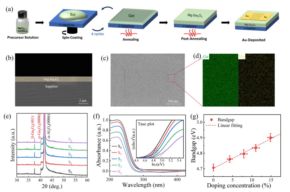
FIG. 1. (a) Schematic diagram of solution-process Mg-doped Ga2O3 device fabrication. Cross-sectional (b) and top-view (c) SEM image, (d) EDS element (Ga and Mg) mapping results of the S1. (e) XRD patterns and (f) absorbance spectra of each film (the insert Tauc plot). (g) The variation regular of bandgap with doping concentration.
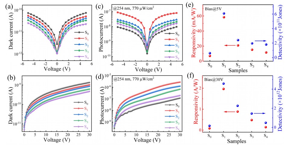
FIG. 2. I–V curves of each device in the dark (a) and (b) and under the 254 nm ultraviolet illumination (c) and (d) at low and high bias, respectively. Parameter R, D_x0005_* of the devices at the voltage of (e) 5 V and (f) 30 V.
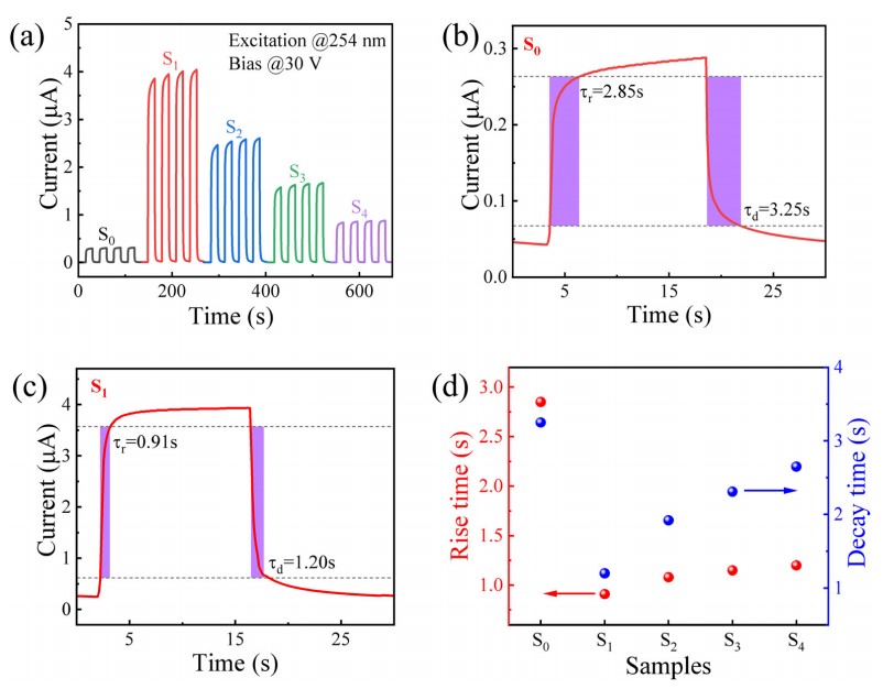
FIG. 3. (a) Dynamic response of the devices under ultraviolet light at a bias of 30 V. Response times of (b) device S0 and (c) device S1. (d) Comparison of response time.
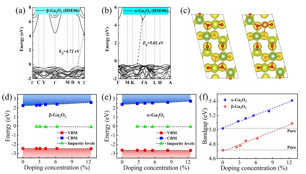
FIG. 4. The band structure of (a) β-Ga2O3 and (b) α-Ga2O3 based on the HSE06 method. (c) The partial charge density distribution of pristine and Mg-doped β-Ga2O3. The comparison of the band offsets and the impurity levels positions of (d) Mg-doped β-Ga2O3 and (e) Mg-doped α-Ga2O3. (f) The fitting relationship of the bandgap of α- and β-Ga2O3 with respect to the linearity of the Mg-doping concentration.
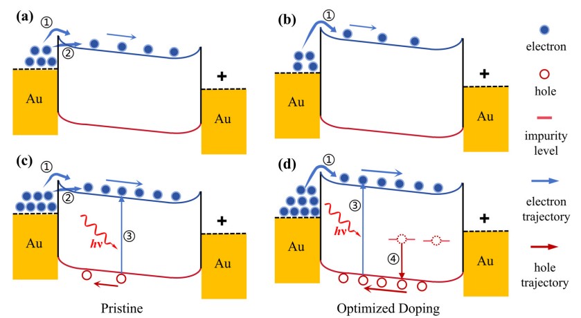
FIG. 5. Schematic energy band diagrams of the MSM structure devices. The pristine (left) and Mg-doped (right) Ga2O3 devices operate separately in the dark condition (a) and (b) and under ultraviolet illumination (c) and (d).
This work investigated the effects of Mg²⁺ doping concentration on the photoelectric properties of Ga₂O₃ thin films using the sol-gel method, tested the photoelectric performance differences of devices under various doping concentrations, and achieved high-performance photodetectors with optimized doping densities. By combining theoretical calculations, the authors analyzed and proposed the intrinsic physical mechanisms behind the performance improvements. This doping research strategy can provide insights for doping with other elements or optimizing other semiconductor materials, offering a promising direction for future semiconductor optoelectronic devices.
Original Article:
doi.org/10.1063/5.0246775
