Paper Sharing
【Domestic Papers】 Beijing University of Technology —— Growth modes of β-Ga₂O₃ on h-BN: Remote epitaxy and van der Waals epitaxy
日期:2025-03-03阅读:880
Researchers from the Beijing University of Technology have published a dissertation titled "Growth modes of β-Ga2O3 on h-BN: Remote epitaxy and van der Waals epitaxy" in Nano Research.
Abstract
Integrating monoclinic gallium oxide (β-Ga2O3) with two-dimensional (2D) hexagonal boron nitride (h-BN) into heterostructures is of significant importance for achieving high-power device applications. The 2D-material-assisted epitaxy provides a straightforward integration method for fabricating β-Ga2O3/h-BN vertical heterostructures. In this work, the β-Ga2O3 films were deposited on both polycrystalline and single-crystalline h-BN layers with different thicknesses, and two growth modes of β-Ga2O3 films on h-BN, remote epitaxy, and van der Waals (vdW) epitaxy, were investigated. The results show that the potential of the sapphire substrate can penetrate the monolayer and bilayer h-BN to obtain the remote epitaxy of β-Ga2O3 films, regardless of the crystallinity of h-BN. The vdW epitaxy of β-Ga2O3 film can be realized on the monocrystalline h-BN substrate. Compared with the conventional and remote epitaxial β-Ga2O3 films on sapphire substrate, the vdW epitaxial β-Ga2O3 films on the single-crystalline h-BN substrate exhibit higher crystallinity. This work indicates that the 2D-material-assisted epitaxy provides a feasible scheme for the heterogeneous integration of β-Ga2O3 films.
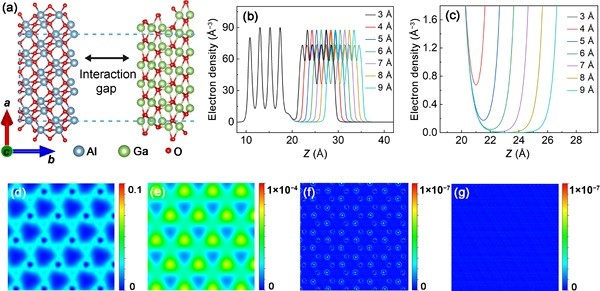
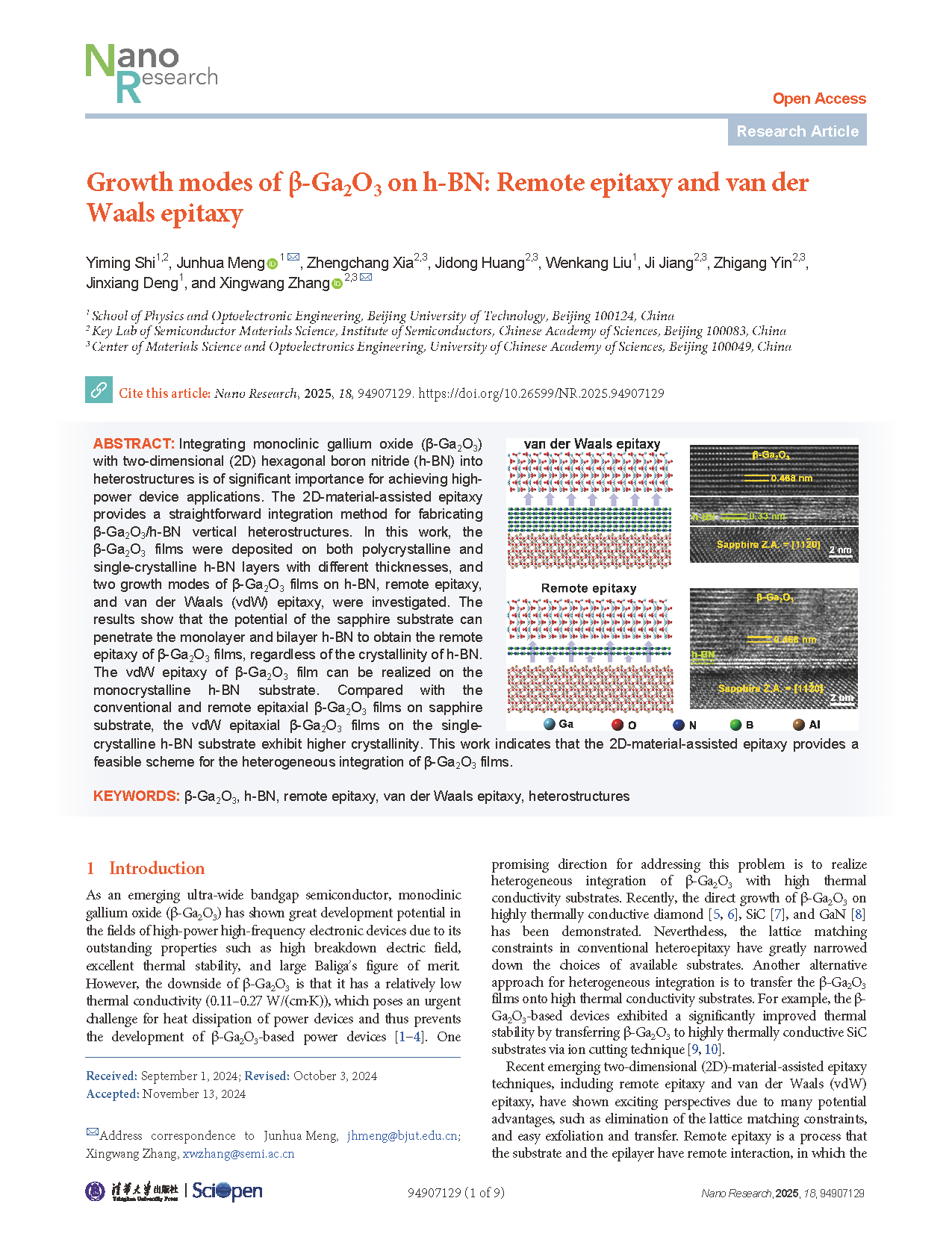
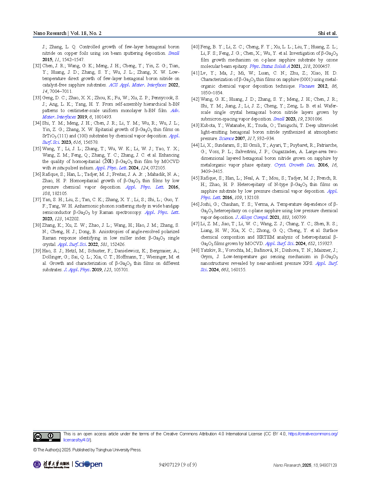
Figure 1(a) Schematic of Al–Ga remote interaction gaps created by different numbers of h-BN layers spaced along the Z-axis of the c-sapphire. (b) DFT calculating electron density along separated slabs of Al-terminated c-sapphire and β-Ga2O3. (c) An enlarged view of the electron density within the gap region in (b). Charge density distribution of the Al-terminated c-sapphire through different interaction gaps equivalent to different numbers of h-BN layers: (d) without h-BN interlayer, (e) monolayer h-BN, (f) bilayer h-BN, and (g) tri-layer h-BN.
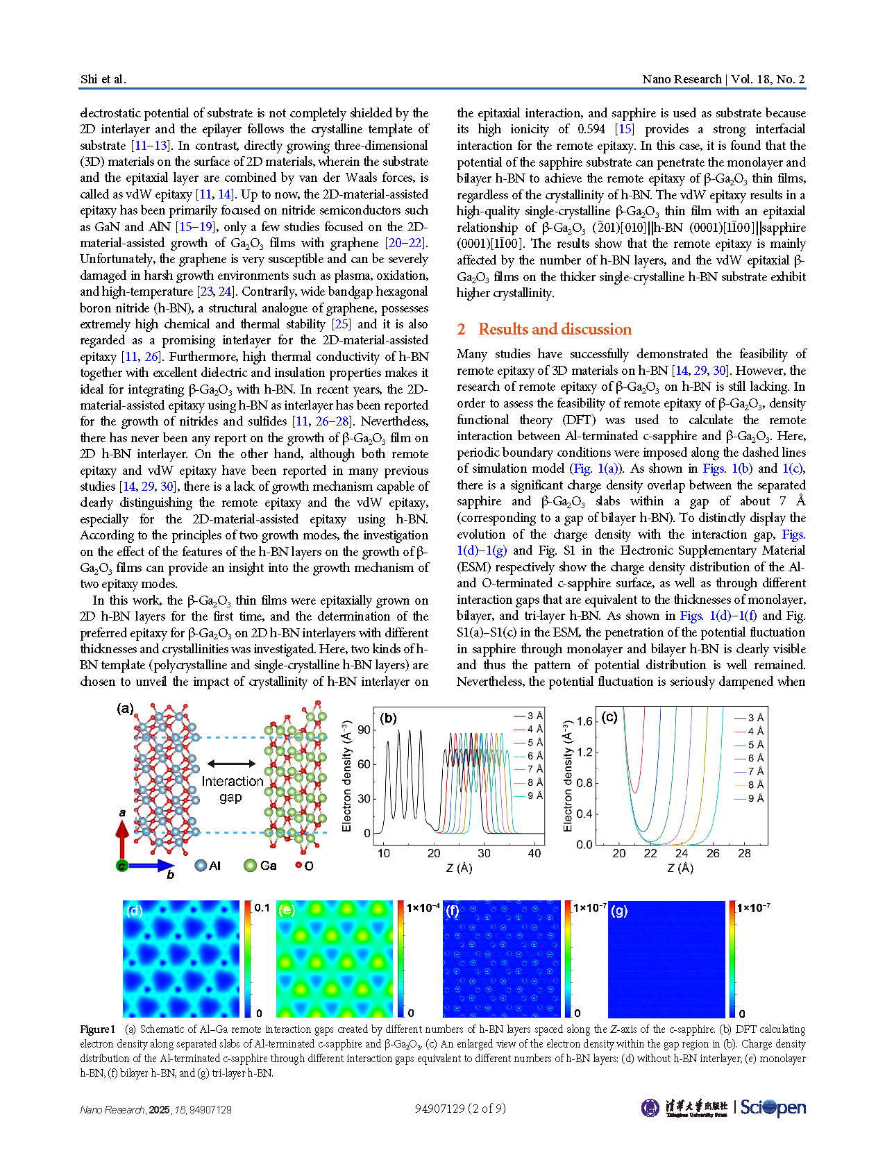
Figure 2. Typical SEM images of IBSD-grown (a) monolayer, (b) bilayer, and (c) tri-layer polycrystalline h-BN on Cu foils. (d) AFM image of the monolayer h-BN transferred onto a sapphire substrate. (e) XPS spectra of B 1s and N 1s core levels of the polycrystalline h-BN. (f) Raman spectra of the polycrystalline h-BN with different layer numbers transferred onto sapphire substrates.
DOI:
doi.org/10.26599/NR.2025.94907129