


Paper Sharing
【International Papers】Researchers from the Polish Academy of Sciences and the Leibniz-Institut für Kristallzüchtung of The electric field influence on Ec-0.18 eV electron trap level in (100)-oriented β-Ga₂O₃ crystals grown by the Czochralski method
日期:2025-03-03阅读:904
Researchers from the Polish Academy of Sciences and the Leibniz-Institut für Kristallzüchtung have published a dissertation titled "The electric field influence on EC-0.18 eV electron trap level in (100)-oriented β-Ga2O3 crystals grown by the Czochralski method" in Applied Physics Letters.
Lead Author Introduction

Piotr Kruszewski
Interests: Electrical characterization of wide bandgap semiconductors (mostly GaN-based materials) and defects analysis by capacitance-based techniques: capacitance-voltage (C-V) in wide range of temperature (77K-700K), temperature dependent current-voltage (I-V), DLTS (Deep Level Transient Spectroscopy) and Laplace DLTS for defect characterization, SiPDR (Single Post Dielectric Resonator) – contactless and on-wafer/structure resistivity analysis, temperature-dependent Hall effect analysis, Hg-probe for non-destructive material analysis, Most structures and devices can be characterized on wafer by the 4-needle probe station (300K only)
Program Support
The work by A. Fiedler was partially funded by the Leibniz-Gemeinschaft project under Grant No. K429/2021. The authors express their gratitude to C. Schafer for contact preparation, A. Kwasniewski for crystal orientation, T. Wurche for crystal cutting as well as Tobias Schulz for critical reading of the present paper, all from Leibniz-Institut für Kristallzüchtung (IKZ), and K.Gibasiewicz for the electrical connection of the diodes from the Institute of High Pressure Physics, Polish Academy of Sciences (IHPP PAS).
Abstract
In this Letter, we demonstrate the application of Deep Level Transient Spectroscopy (DLTS) and Laplace DLTS (L-DLTS) techniques to unintentionally doped β-Ga2O3 crystals grown by the Czochralski method. It is clearly shown that the capacitance signal associated with the electron emission from a trap level previously identified in the literature as E14 and characterized by an activation energy of 0.18 eV is found to be a superposition of electron emissions from two closely spaced energy levels. Furthermore, we noted that the corresponding L-DLTS signal splits into two well separated components with activation energies of 196 and 209 meV, and the splitting occurs as the electric field in the space charge region of a Schottky diode exceeds 2 × 10⁷ V/m (0.2 MV/cm). Additionally, a strong dependency of DLTS and L-DLTS signals on the electric field strength and resulting enhancement of the electron emission from these two trap states agree well with the 1D Poole–Frenkel (PF) model, suggesting donor-like behavior of both states. Finally, we found that the barrier height for thermal emission of the electrons is significantly reduced in our samples by 121 meV due to the PF effect for experimental conditions corresponding to an electric field of 3.5 × 10⁷ V/m (0.35 MV/cm).
Experimental Diagram
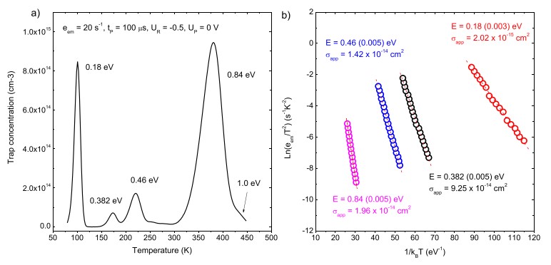
FIG. 1. (a) A DLTS spectrum for UID CZ-grown β-Ga2O3 sample for a rate window of 20 s-1 and (b) corresponding activation energies and apparent capture cross sections determined from Arrhenius plots for all trap levels detected by DLTS.
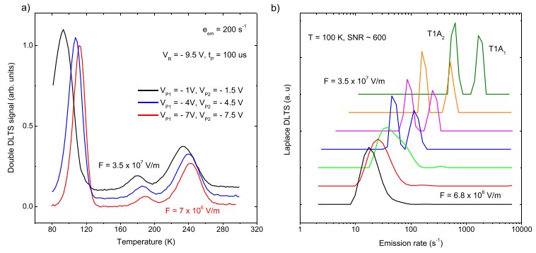
FIG. 2. (a) Field dependent D-DLTS spectra measured for CZ-grown UID β-Ga2O3 samples with the signal normalized to the low temperature peak intensity and shifted along the Y-axis and (b) Double L-DLTS spectra obtained from capacitance transients, measured in different regions of the depletion region of the Schottky diode, for a trap with EC-0.18 eV
DOI:
doi.org/10.1063/5.0251567


