Paper Sharing
【International Papers】Optimization of fin-slanted angles for enhanced electrical performance in lateral β-Ga₂O₃ MOSFETs
日期:2025-03-04阅读:851
Researchers from the National University of Singapore have published a dissertation titled "Optimization of fin-slanted angles for enhanced electrical performance in lateral β-Ga2O3 MOSFETs" in Applied Physics Letters.

Corresponding Author Introduction

Dr. Gong Xiao is currently an Associate Professor in the ECE Department of the National University of Singapore (NUS). He obtained his Ph. D Degree from NUS and was a Visiting Scientist at MIT in the year of 2014. His research interest includes advanced transistors and emerging memories for in-memory computing, monolithic 3D integration, opto-electronic integrated circuits and their applications in quantum technology, as well as ultra-high frequency and ultra-wide bandgap device technology. He has more than 330 publications in international journals and conferences, including more than 80 papers in IEDM and VLSI Symposium. He is the Editor of IEEE Electron Device Letters.
Article Abstract
In this work, the influence of fin-slanted angles (α) on the electrical performance of lateral β-Ga2O3 MOSFETs was investigated through a combination of experiments and Sentaurus TCAD simulations. The fin-slanted devices demonstrated enhancement-mode characteristics with an on/off ratio of around 107. The increment in α resulted in improved drain-to-source current (IDS) and extrinsic transconductance (Gm). The voltage-blocking performance also showed significant enhancement with increasing α due to the mitigation of edge crowding, achieving a 40% increase in the breakdown voltage (VBR) for devices with an α of 15° and gate-to-drain length (LGD) of 10 μm. A detailed simulation analysis of the electric field distribution within the fin at the gate electrode edge identified an optimal α of approximately 25°, which effectively mitigates electric field crowding and has the potential to enhance the DC performance of the MOSFETs. These findings highlight the critical role of fin-slanted angle optimization in advancing the performance of lateral β-Ga2O3 MOSFETs, positioning them as promising candidates for next-generation power electronics.
Experimental Diagram
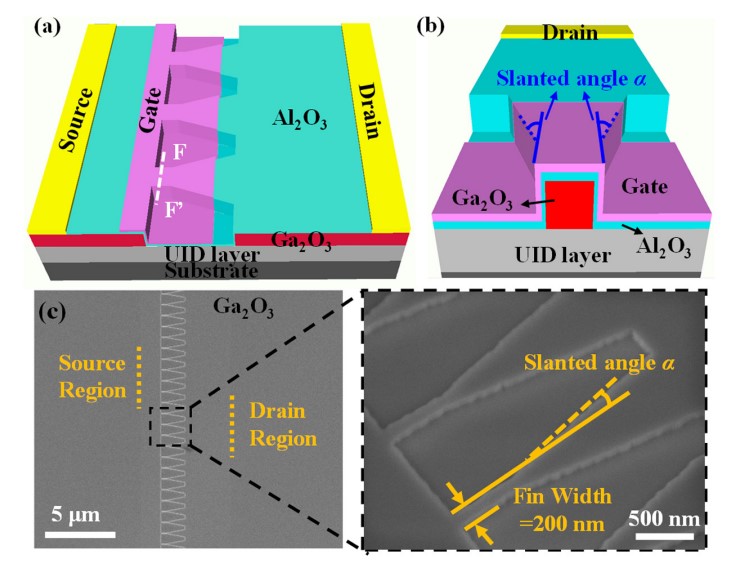
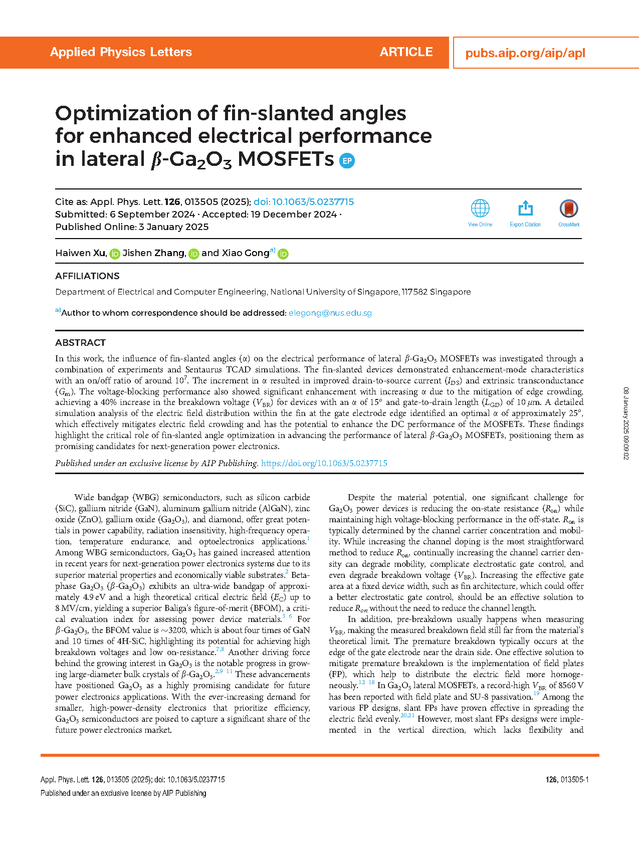
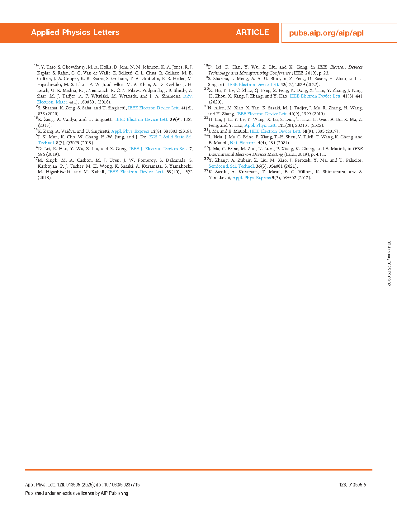
FIG. 1. (a) 3D schematic of the fabricated β-Ga2O3 MOSFET with the slanted-fin structure. (b) The sidewall view of the fin structure, taken along the line FF’and facing the drain side. Each fin consists of an initial straight section near the source, with the remaining portion slanted to two sides at a defined angle, denoted as α. (c) Top-view SEM image of the fin structure and the zoomed-in image of the channel region with slanted-fin structure after the fin-etch step, showing the fin dimensions.
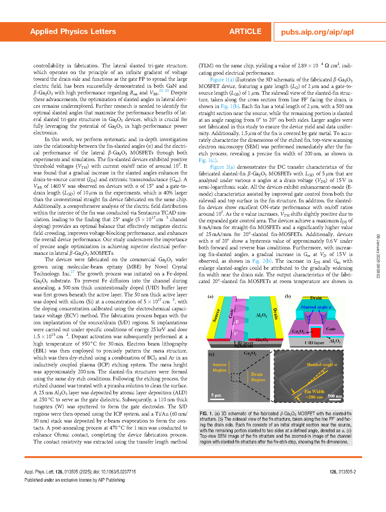
FIG. 2. (a) Semi-logarithmic scale transfer characteristics of the lateral slanted-fin β-Ga2O3 MOSFETs with various α angles. The inset shows the hysteresis of the 20°-slanted fin device. (b) Gm vs VG characteristics of the fabricated β-Ga2O3 MOSFETs. (c) Output characteristics of the fabricated β-Ga2O3 MOSFETs with 20° slanted angle. (d) SS of the fabricated devices with varying slanted angles.
DOI:
doi.org/10.1063/5.0237715