Paper Sharing
【International Papers】κ/β-Ga₂O₃ Type-II Phase Heterojunction
日期:2025-03-07阅读:896
Researchers from the King Abdullah University of Science and Technology (KAUST) have published a dissertation titled "κ/β-Ga2O3 Type-II Phase Heterojunction " in Advanced Materials.
Abstract
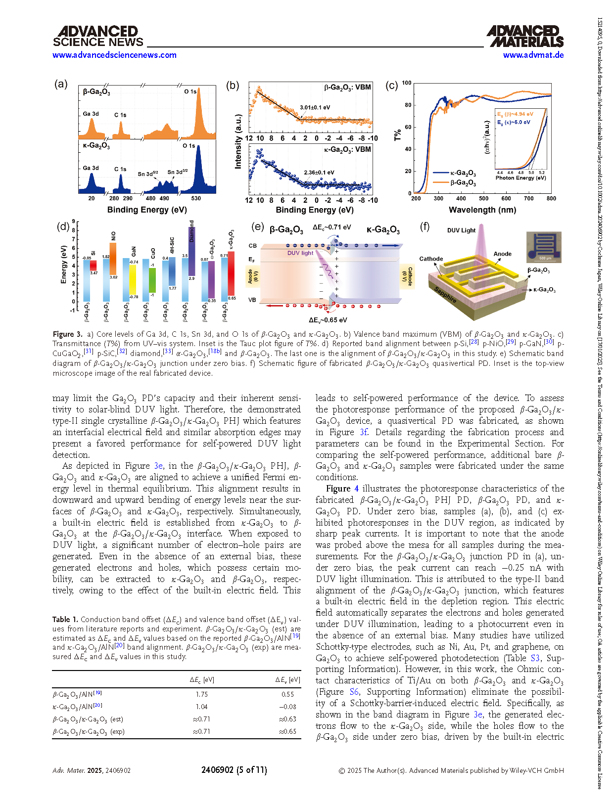
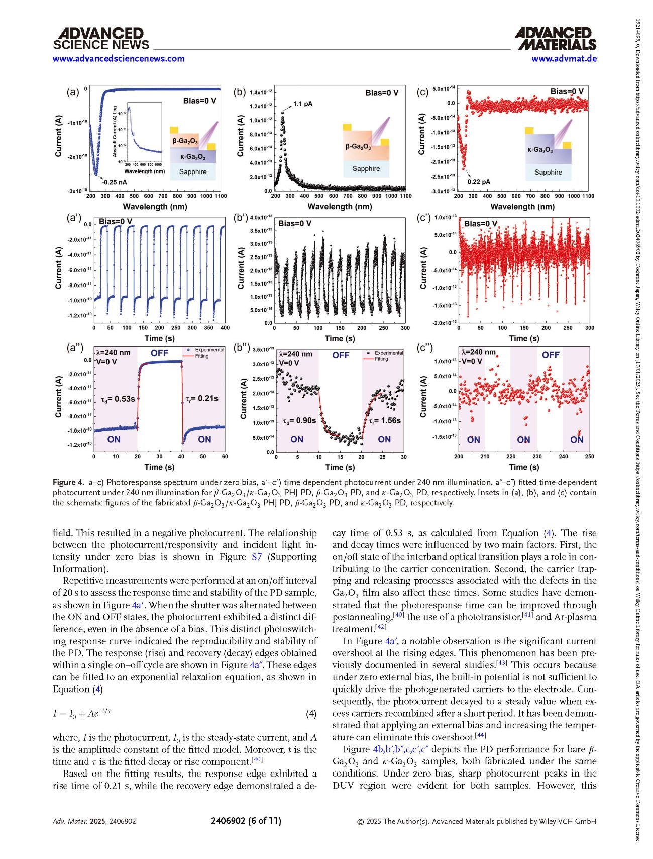
Ultrawide-bandgap gallium oxide (Ga2O3) holds immense potential for crucial applications such as solar-blind photonics and high-power electronics. Although several Ga2O3 polymorphs, i.e., α, β, γ, δ, ε, and κ phases, have been identified, the band alignments between these phases have been largely overlooked due to epitaxy challenges and inadvertent neglect. Despite having similar stoichiometry, heterojunctions involving different phases may exhibit band offsets. Here, β-Ga2O3/κ-Ga2O3-stacked “phase heterojunction” is demonstrated experimentally. This phase heterojunction has a sharp and well-defined interface, and subsequent measurements reveal an unbeknown type-II band alignment with significant valence/conduction band offsets of ≈0.65 eV/0.71 eV. This alignment is promising for self-powered deep ultraviolet (DUV) signal detection, necessitating an internal electric field near the junction and matching the absorption properties for effective electron–hole separation. The fabricated phase heterojunction photodetector displays a responsivity of three orders of magnitude higher at 17.8 mA W−1, with improved response times (rise time ≈0.21 s, decay time ≈0.53 s) under DUV illumination and without external bias in comparison to the bare β-Ga2O3 and κ-Ga2O3 photodetectors, confirming the strong interfacial electrical field. This study provides profound insight into Ga2O3/Ga2O3 heterojunction interfaces with different polymorphs, allowing the use of phase heterojunctions to advance electronic device applications.
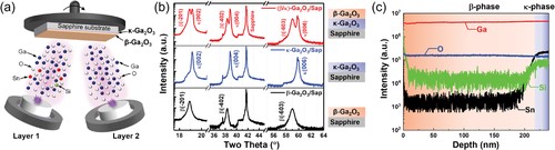
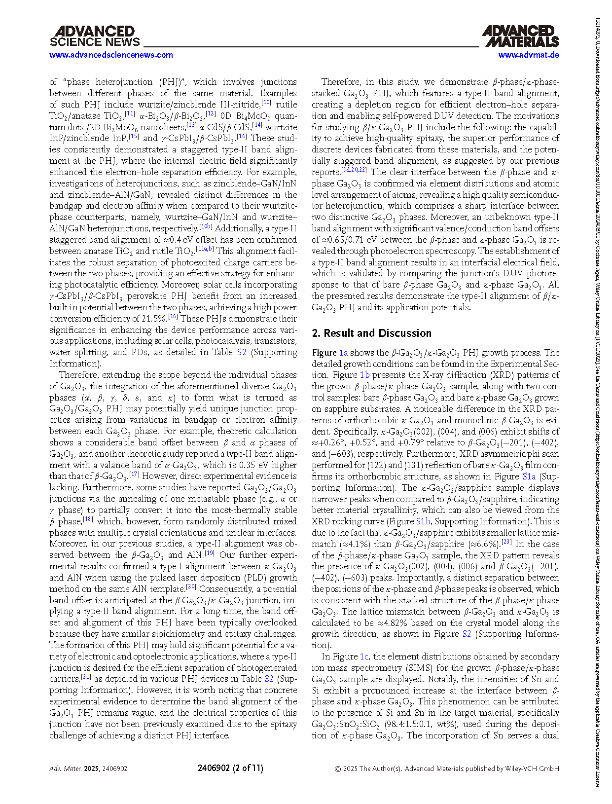
Figure 1. a) Schematic figure of β-phase/κ-phase Ga2O3 PHJ growth. b) X-ray diffraction (XRD) patterns of β-phase Ga2O3, κ-phase Ga2O3, and β-phase/κ-phase Ga2O3 grown on sapphire substrate. c) Secondary ion mass spectrometry (SIMS) profile distribution of Ga, O, Si, and Sn elements of β-phase/κ-phase Ga2O3 sample.
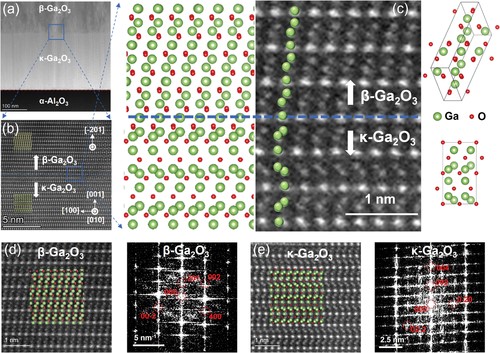
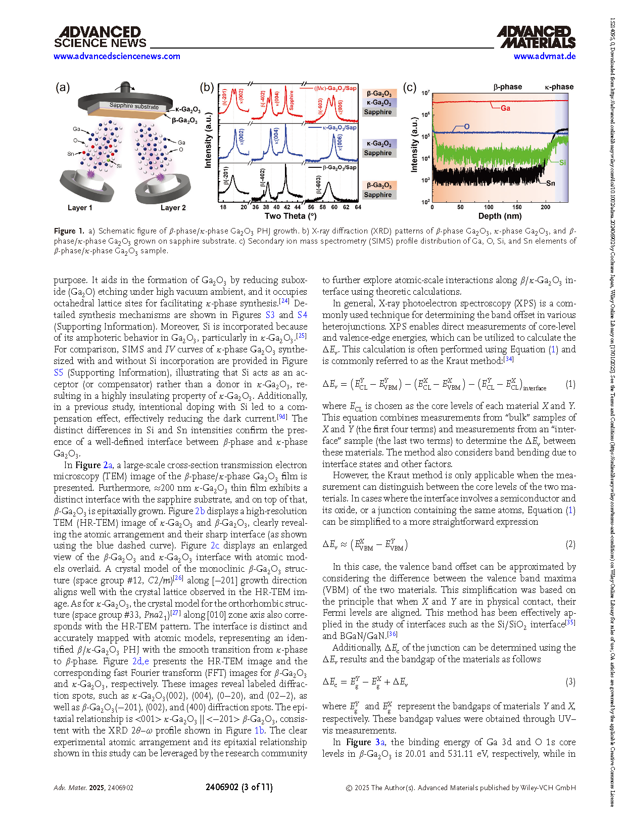
Figure 2. a) Large-scale cross-sectional transmission electron microscopy (TEM) of β-phase/κ-phase Ga2O3 grown on sapphire substrate. b) High-resolution TEM (HR-TEM) image of β-phase/κ-phase Ga2O3 interface. c) Enlarged view of the β-Ga2O3 and κ-Ga2O3 interface with atomic models overlaid, illustrating the clear, sharp, and well-defined interface. Atomic arrangement and fast Fourier transform (FFT) images of d) β-Ga2O3 and e) κ-Ga2O3.
DOI:
doi.org/10.1002/adma.202406902