Paper Sharing
【Member Papers】Xidian University Haoyue&Han Genquan Team —— Highly Stable Electronics Based on β-Ga₂O₃ for Advanced Memory Applications
日期:2025-03-07阅读:963
Researchers from the Xidian University have published a dissertation titled "Highly Stable Electronics Based on β-Ga2O3 for Advanced Memory Applications" in Advanced Science.
Program Support
The authors acknowledge support from the China Postdoctoral Science Foundation (2023M742732), thePostdoctoral Fellowship Program of CPSF under Grant Number GZC20241303, theFundamental Research Funds for the Central Universities (XJSJ24100), the National Natural Science Foundation of China (Grant No. 62404176, 62025402, 62090033, 92364204, 9226420, 12175298, and 62293522)and the Major Program of Zhejiang Natural Science Foundation (Grant No. LDT23F04024F04). The authors thank beamlines BL17B1, BL16U1, BL06B, BL19U2, BL02U2, and BL01B1 staff at the SSRF and User Experiment Assist System of SSRF for their help. The authors thank Professor Chang-Tai Xia's group from the Key Laboratory of Materials for High Power Laser Shanghai Institute of Optics and Fine Mechanics, Chinese Academy of Sciences for providing the β-Ga2O3 single crystal bulk. And Chang-Tai Xia acknowledges the National Natural Science Foundation of China (No. 51972319) and the Science and Technology Commission of Shanghai Municipality (No. 19520744400).
Abstract
Wide-bandgap (WBG) semiconductors are at the forefront of driving innovations in electronic technology, perpetuating Moore's Law and opening up new avenues for electronic devices. Although β-Ga2O3 has attracted extensive research interest in advanced electronics, its high-temperature and high-speed volatile memory applications in harsh environment has been largely overlooked. Herein, a high-performance hexagonal boron nitride (h-BN)/β-Ga2O3 heterostructure junction field-effect transistor (HJFET) is fabricated, exhibiting an off-state current as low as ≈10 fA, a high on/off current ratio of ≈108, a low contact resistance of 5.6 Ω·mm, and an impressive field-effect electron mobility of 156 cm2 (Vs)−1. Notably, the current h-BN/β-Ga2O3 HJFET exhibits outstanding thermal reliability in the ultra-wide temperature range from 223 to 573 K, as well as long-term environmental stability in air, which confirms its inherent capability of operation in harsh environments. Moreover, the h-BN/β-Ga2O3 HJFET demonstrates successful applications for accelerator-in-memory computing fields, including dynamic random-access memory structure and neural network computations. These superior characteristics position β-Ga₂O₃-based electronics as highly promising for applications in extreme environments, with particular relevance to the automotive, aerospace, and sensor sectors.
Experimental Section
Device Fabrication
In this work, the β-Ga2O3 bulk single crystal with 0.05 mol % Ta doping was used. It exhibits an active electron concentration of 1.4 × 1018 cm−3 measured by Hall effect and electrical resistivity tests. Subsequently, β-Ga2O3 flakes were exfoliated mechanically from β-Ga2O3 bulk by commercial Scotch tape and transferred onto 110 nm SiO2/p++-Si substrate. Then, the electron-beam lithography (EBL) process was used to pattern the source/drain regions, followed by the development, e-beam evaporation, and lift-off processes. The stack metal of Ti/Al/Ni/Au (20/100/60/80 nm) was chosen to use as a source/drain electrode. And an RTA process in a high purity N2 ambient was also carried out at 470 °C for 1 min to improve electrode/channel contact. After the fabrication of a two-terminal β-Ga2O3 device, the mechanically exfoliated h-BN flake was precisely transferred to the top of the target β-Ga2O3 channel as the gate dielectric layer using a poly (dimethylsiloxane) transfer method. Finally, the top gate composed of Ti/Au (10/70 nm) was defined via a second EBL, metallization, and lift-off processes to finish the fabrication of h-BN/β-Ga2O3 HJFET.
Microscopic and Electrical Characterizations
The crystalline structure of β-Ga2O3 bulk single crystal was obtained by the Synchrotron-based GIXRD which uses X-ray with a wavelength of 0.6887 Å. The Raman spectrum was investigated using a commercial Raman spectrometer (Horiba Jobin Yvon LabRAM HR800) equipped with an excitation wavelength of 532 nm. The β-Ga2O3 flakes structural analysis was analyzed using HR-TEM (Talos F200X). The thicknesses of h-BN and β-Ga2O3 flakes were determined via AFM (Bruker Dimension Icon). The all-electrical measurements were conducted by using a semiconductor analyzer (Agilent B1500A).
Summary
In summary, a h-BN/β-Ga2O3 HJFET has been fabricated with a low Ioff of ≈10 fA, a high Ion/Ioff of ≈108, a low Rc of 5.6 Ω·mm, and a high μfe of 156 cm2 (Vs)−1. Importantly, the obtained h-BN/β-Ga2O3 HJFET shows not only good thermal reliability in a temperature range of 223–573 K but also high environmental stability even after 18 months. Besides, the h-BN/β-Ga2O3 HJFET can also be used successfully in accelerator-in-memory computing fields including DRAM and neural network computation applications. This work provides a new perspective for the development of next-generation nanoelectronics.
Graphic Abstract
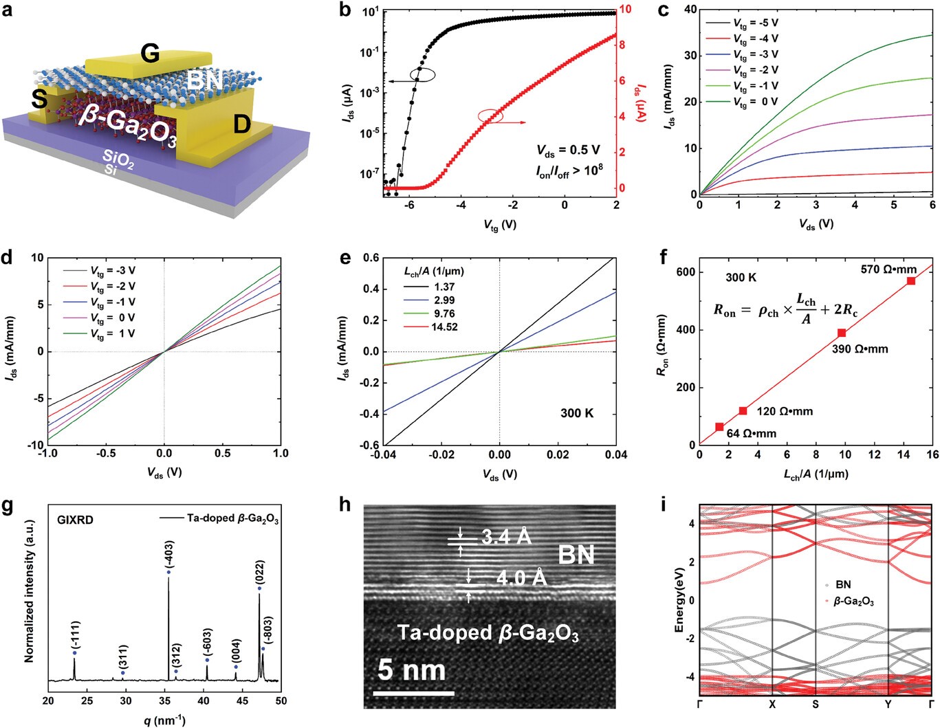
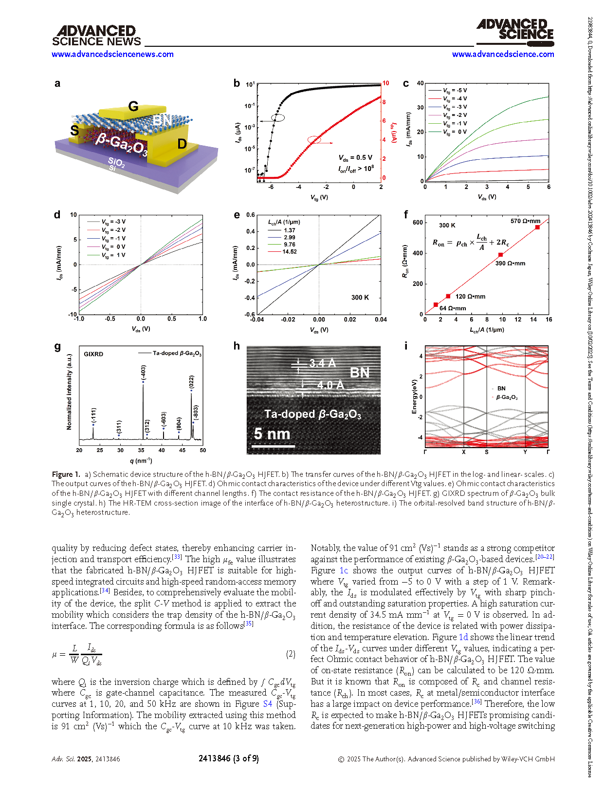
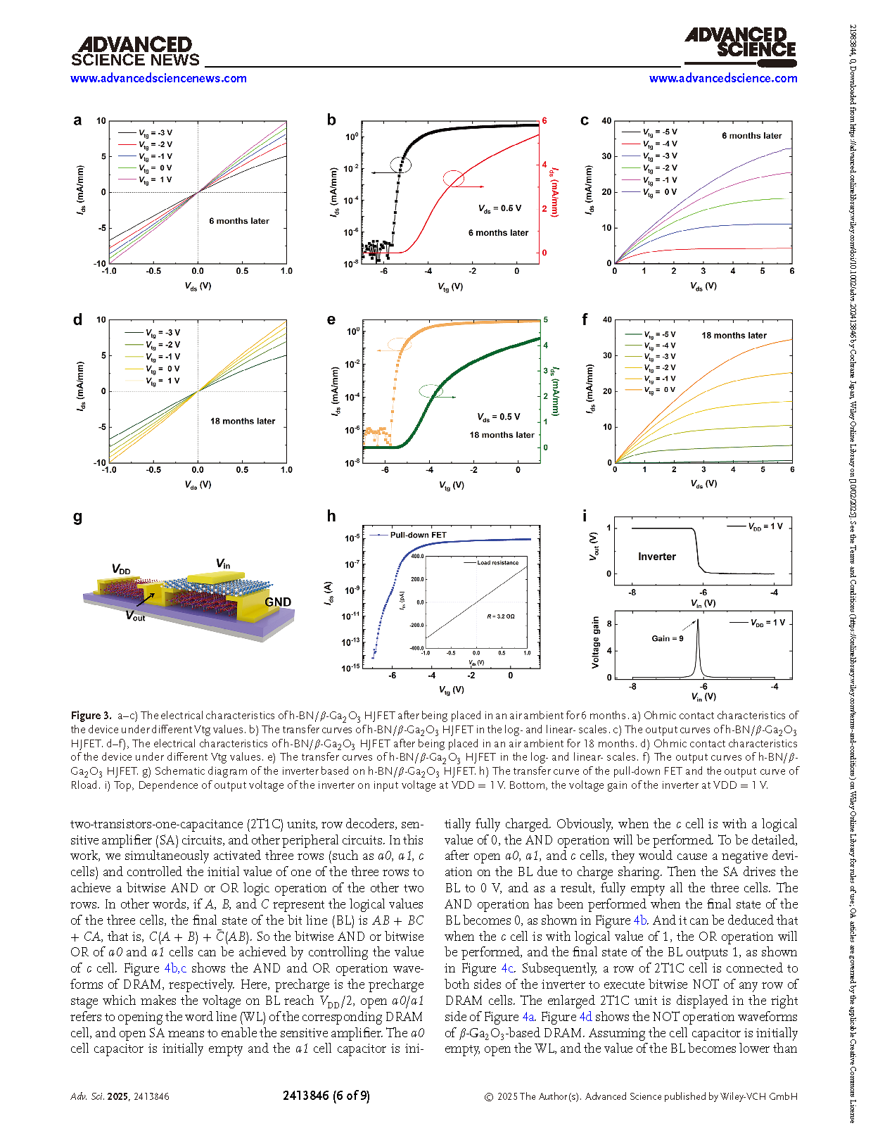
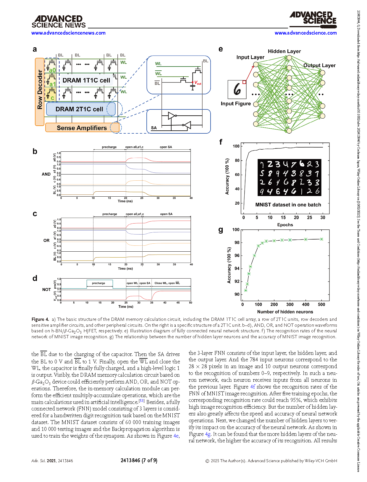
Figure 1. a) Schematic device structure of the h-BN/β-Ga2O3 HJFET. b) The transfer curves of the h-BN/β-Ga2O3 HJFET in the log- and linear- scales. c) The output curves of the h-BN/β-Ga2O3 HJFET. d) Ohmic contact characteristics of the device under different Vtg values. e) Ohmic contact characteristics of the h-BN/β-Ga2O3 HJFET with different channel lengths. f) The contact resistance of the h-BN/β-Ga2O3 HJFET. g) GIXRD spectrum of β-Ga2O3 bulk single crystal. h) The HR-TEM cross-section image of the interface of h-BN/β-Ga2O3 heterostructure. i) The orbital-resolved band structure of h-BN/β-Ga2O3 heterostructure.
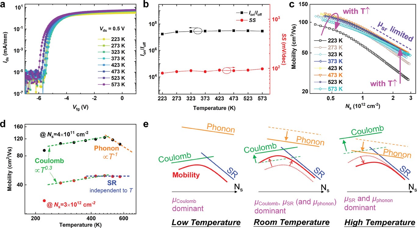
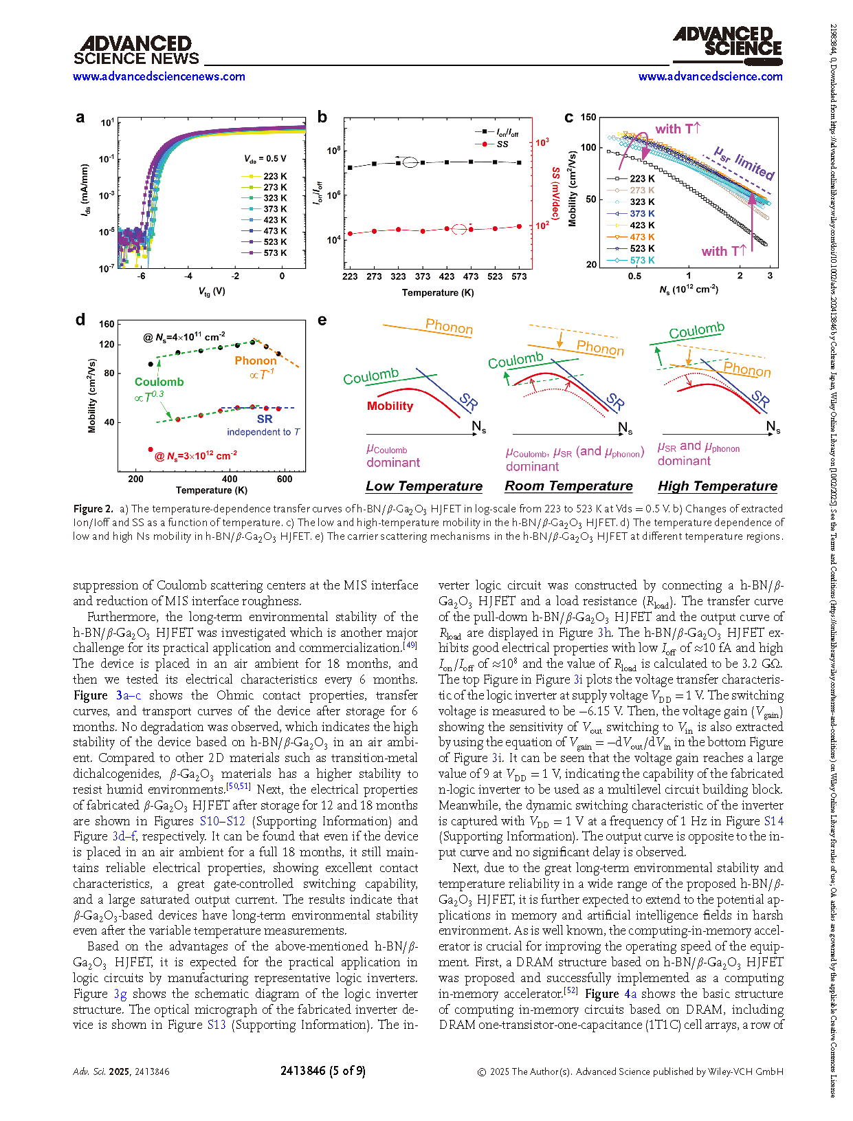
Figure 2. a) The temperature-dependence transfer curves of h-BN/β-Ga2O3 HJFET in log-scale from 223 to 523 K at Vds = 0.5 V. b) Changes of extracted Ion/Ioff and SS as a function of temperature. c) The low and high-temperature mobility in the h-BN/β-Ga2O3 HJFET. d) The temperature dependence of low and high Ns mobility in h-BN/β-Ga2O3 HJFET. e) The carrier scattering mechanisms in the h-BN/β-Ga2O3 HJFET at different temperature regions.
DOI:
doi.org/10.1002/advs.202413846