Paper Sharing
【Domestic Papers】 China University of Geosciences —— High-performance Ga₂O₃-based solar-blind UV photodetectors developed with low fabricating and operating temperature
日期:2025-03-11阅读:811
Researchers from the China University of Geosciences have published a dissertation titled "High-performance Ga2O3-based solar-blind UV photodetectors developed with low fabricating and operating temperature" in High-performance Ga2O3-based solar-blind UV photodetectors developed with low fabricating and operating temperature.
Abstract
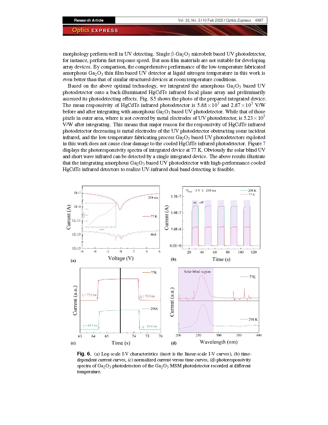
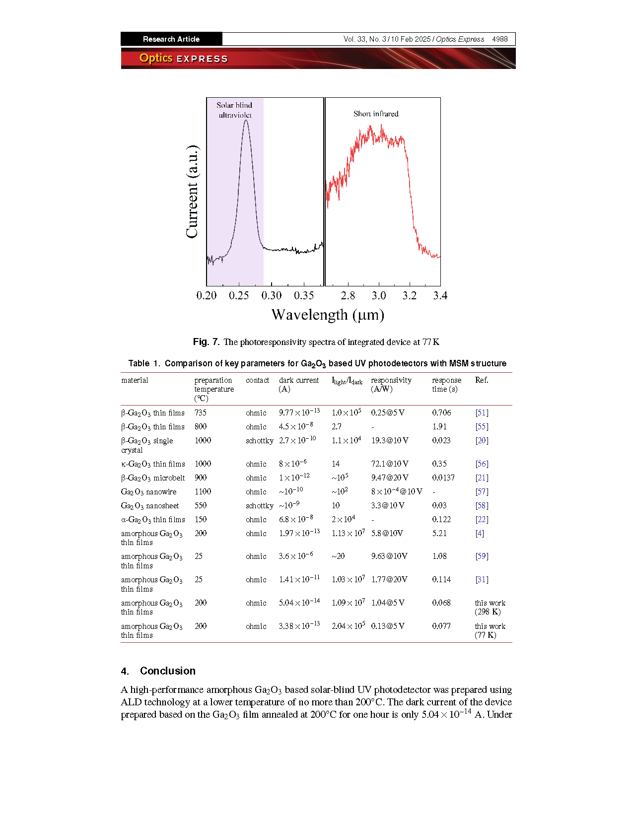
Infrared and ultraviolet dual-band integrated detectors are among the most important development trends in photodectors. To be compatible with the low operating and mild fabricating temperature for cooled infrared detectors, it is crucial to develop low-temperature operating UV photodetectors with mild fabricating conditions. In this work, we developed amorphous Ga2O3-based metal-semiconductor-metal solar-blind UV photo-detectors with a low temperature process no higher than 200°C. The photodetectors fabricated with the low-temperature annealed ALD-Ga2O3 thin films exhibit an ultra-low dark current of 5.04 × 10⁻¹⁴ A, high photo-to-dark current ratio of 1.09 × 10⁷, high detectivity of 6.5 × 10¹⁵ Jones and responsivity of 1.04 A/W at bias of 5 V. The rise and decay times are less than 70 ms. The changes of oxygen vacancy defects and crystallization region are probably the main reasons. Besides, the prepared photodetectors represent the photo-to-dark current ratio of 2.04 × 10⁵, detectivity of 4.8 × 10¹⁴ Jones, and responsivity of 0.13 A/W at liquid nitrogen temperature. Further, the optimal UV photodetectors were integrated with HgCdTe infrared photodetector realizing solar blind UV and short infrared detecting by a single device. This work provides some ideas for exploiting the low-temperature fabricating process of Ga2O3-based UV photodetectors and widening its low-temperature application scenarios. It also lays a foundation for integrating with a cooled infrared detector.
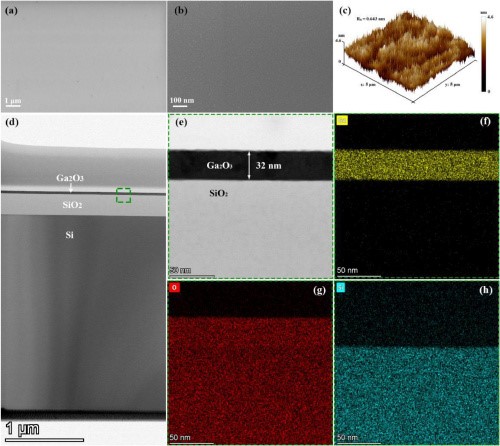
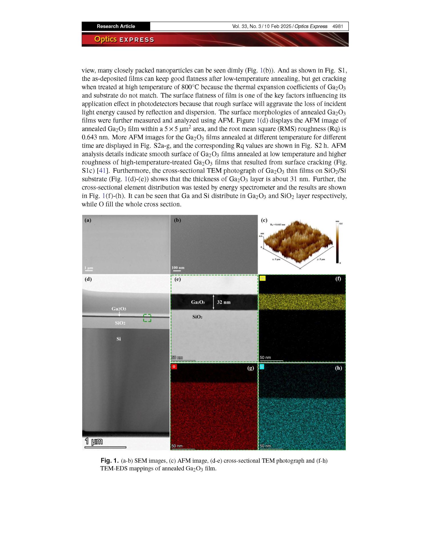
Fig. 1. (a-b) SEM images, (c) AFM image, (d-e) cross-sectional TEM photograph and (f-h) TEM-EDS mappings of annealed Ga2O3 film.
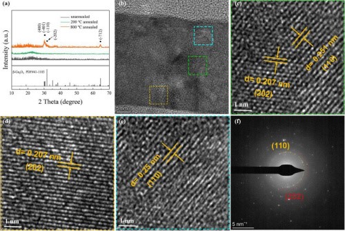
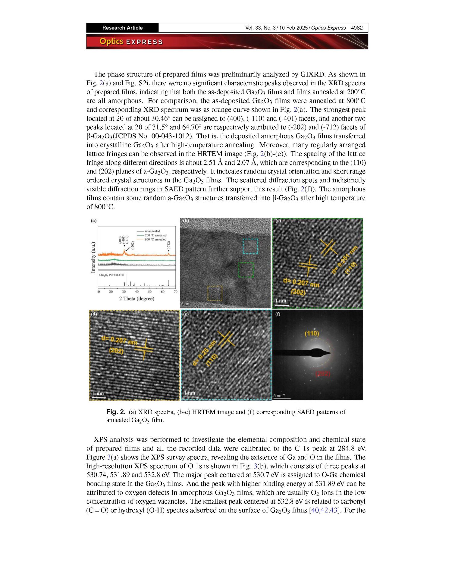
Fig. 2. (a) XRD spectra, (b-e) HRTEM image and (f) corresponding SAED patterns of annealed Ga2O3 film.
DOI:
doi.org/10.1364/OE.542848