Paper Sharing
【Domestic Papers】Songshan Lake Materials Laboratory——Probing interfacial states in β-Ga₂O₃/SiO₂ TFTs for high-response broad-band photodetection
日期:2025-03-12阅读:935
Researchers from the Songshan Lake Materials Laboratory have published a dissertation titled "Probing interfacial states in β-Ga2O3/SiO2 TFTs for high-response broad-band photodetection" in Applied Physics Letters.
Researchers Introduction
Located in Dongguan, one of the main cities in the Guangdong-Hong Kong-Macao Greater Bay Area, Songshan Lake Materials Laboratory (SLAB) started construction on December 22, 2017 and completed registration in April, 2018. As one of the first Guangdong provincial laboratories, SLAB consists of four core sections: the Frontier Research Center, the Public Technology Platform and Large-scale Scientific Facilities, the Model Factory for Innovation, and the South Bay Interdisciplinary Science Center, which will form the entire chain of "frontier basic research → applied basic research → industrial technology research → industrial transformation". It is expected to become an internationally recognized southern base for new materials research and development, an important component of China’s materials research, and a new window of interdisciplinary cooperation in the Guangdong-Hong Kong-Macao Greater Bay Area.
Program Support
This work was supported by the National Natural Science Foundation of China (Grant Nos. 12174275, 62174113, and 62204169), Youth Innovation Team of colleges and universities in Shandong Province (Grant No. 2022KJ223), and Shandong Provincial Natural Science Foundation (Grant No. ZR2021QF020)
Abstract
Mechanically exfoliated β-Ga2O3 flakes preserve bulk material's single crystallinity for easy integration but suffer from interfacial defects that greatly influence device performance. In this paper, we report a quantitative characterization of interfacial states in phrase β-Ga2O3/SiO2 thin-film transistors and then propose their beneficial application in achieving high-response broad-band photodetection. Photo-excited charge collection spectroscopy technique was employed to probe the interfacial states, revealing a substantial density (∼4 × 1012 cm−2 eV−1) of deep-level states ranging from 2.5 to 3.7 eV below the conduction band. Intriguingly, a photoresponsivity as high as 2 × 10⁴ A/W was achieved via utilizing these interfacial states, along with the tunable broad-band response ranging from 335 to 496 nm. This research enhances both the well-industrialized silicon devices and the emerging β-Ga2O3 technologies. Furthermore, it introduces a profound concept: defects, once seen as flaws, can be assets when their characteristics are thoroughly understood.
Summary
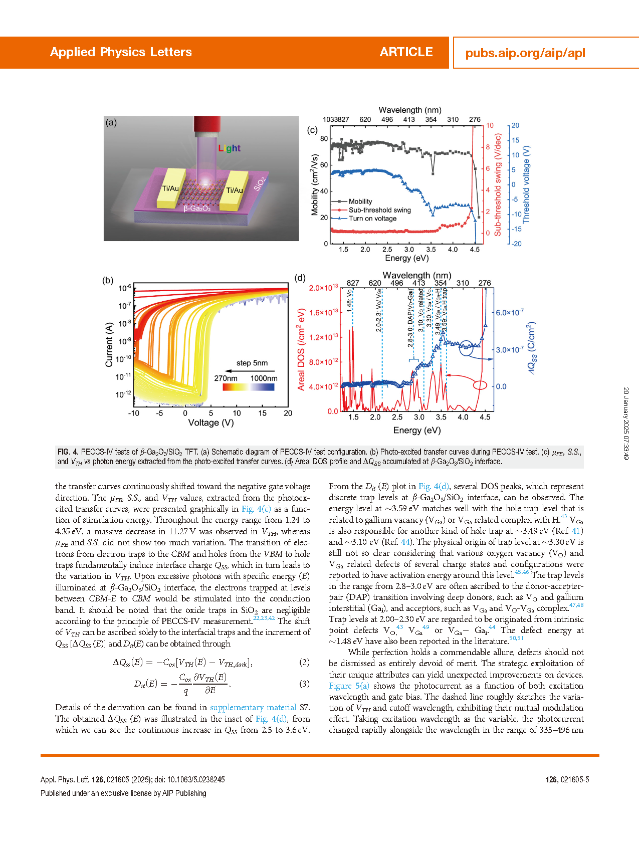
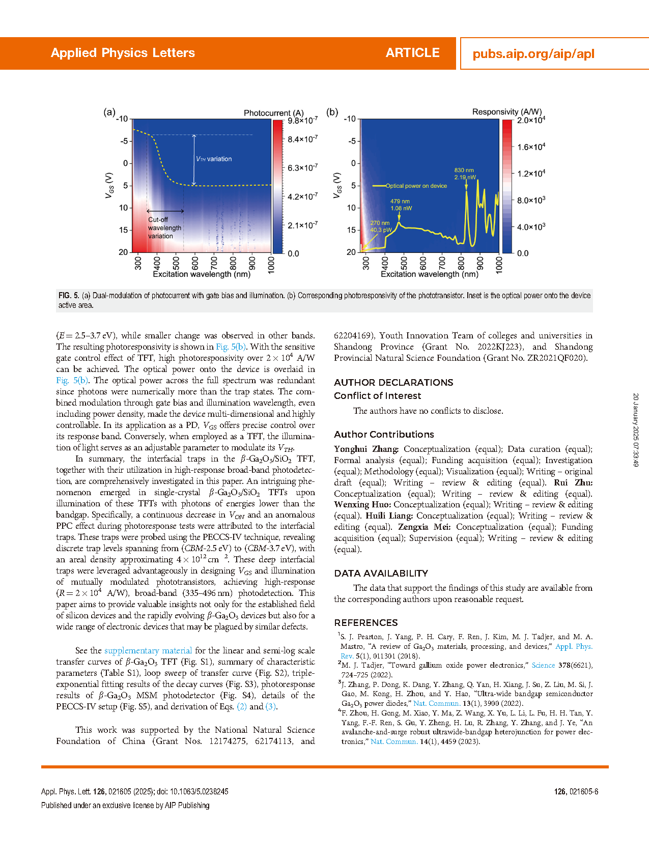
In summary, the interfacial traps in the β-Ga2O3/SiO2 TFT, together with their utilization in high-response broad-band photodetection, are comprehensively investigated in this paper. An intriguing phenomenon emerged in single-crystal β-Ga2O3/SiO2 TFTs upon illumination of these TFTs with photons of energies lower than the bandgap. Specifically, a continuous decrease in VON and an anomalous PPC effect during photoresponse tests were attributed to the interfacial traps. These traps were probed using the PECCS-IV technique, revealing discrete trap levels spanning from (CBM-2.5eV) to (CBM-3.7eV), with an areal density approximating 4 × 1012cm-2. These deep interfacial traps were leveraged advantageously in designing VGS and illumination of mutually modulated phototransistors, achieving high-response (R=2 × 10⁴ A/W), broad-band (335–496nm) photodetection. This paper aims to provide valuable insights not only for the established field of silicon devices and the rapidly evolving β-Ga2O3 devices but also for a wide range of electronic devices that may be plagued by similar defects.
Graphic Abstract
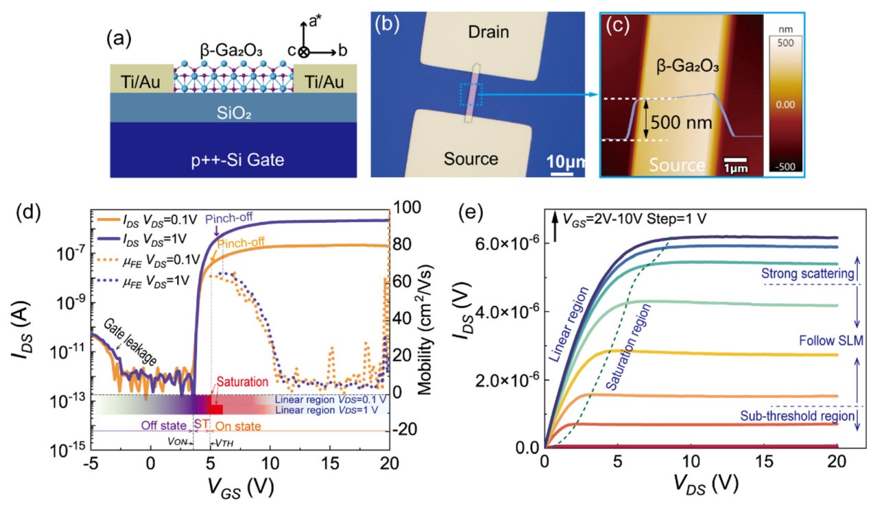
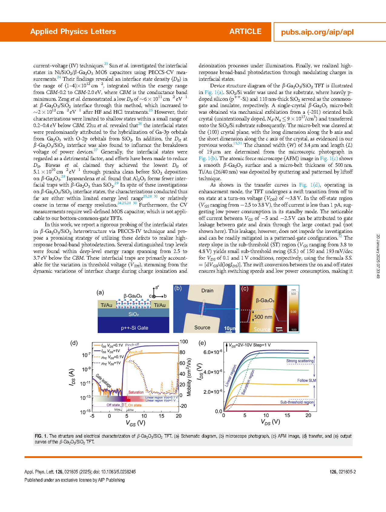
FIG. 1. The structure and electrical characterization of β-Ga2O3/SiO2 TFT. (a) Schematic diagram, (b) microscope photograph, (c) AFM image, (d) transfer, and (e) output curves of the β-Ga2O3/SiO2 TFT.
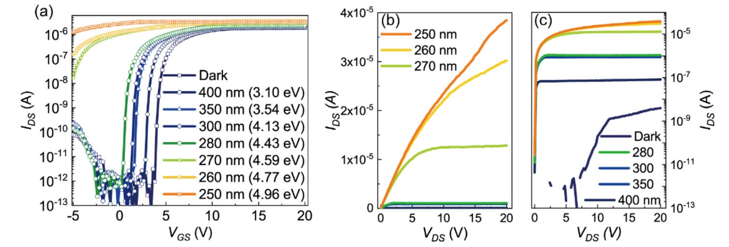
FIG. 2. Electrical test of the β-Ga2O3/SiO2 TFT under illumination. (a) Transfer curves with VDS = 1 V, output curves with VGS = 3 V under light illumination in (b) linear and (c) logarithmic scale.
DOI:
https://doi.org/10.1063/5.0238245