Paper Sharing
【Member Papers】 Westlake University —— Single-Crystalline β-Ga₂O₃ Homoepitaxy on a Near Van der Waals Surface of (100) Substrate
日期:2025-03-13阅读:945
Researchers from the Westlake University have published a dissertation titled "Single-Crystalline β-Ga2O3 Homoepitaxy on a Near Van der Waals Surface of (100) Substrate" in Advanced Science.
Acknowledgements
The authors thank the Instrumentation and Service Center for Physical Sciences, Westlake Center for Micro/Nano Fabrication and Instrumentation, and Instrumentation Service Center for Molecular Sciences at Westlake University for help with characterizations. This work was supported by Westlake Education Foundation. The work of Z.Y. was supported by the Guangdong Major Project of Basic Research under Project No. 2021B0301030003.
Background
Gallium oxide (Ga₂O₃) has attracted considerable attention due to its promising potential as a wide-bandgap semiconductor, particularly for power devices that require high breakdown voltage and low on-resistance. These characteristics position Ga₂O₃ as a strong contender to silicon carbide (SiC), owing to its favorable material properties. Ga₂O₃ exists in five polymorphic forms, with β-Ga₂O₃ being the most thermally stable and suitable for melt growth, enabling the production of large-diameter, low-cost substrates analogous to silicon. Currently, 6-inch β-Ga₂O₃ wafers in the (100) orientation have been successfully produced, and further advances are expected to increase wafer sizes. However, the homoepitaxial growth of β-Ga₂O₃ on on-axis (100) substrates is challenging due to the high density of twin boundaries (TBs) and stacking faults (SFs) in the epitaxial layer, which negatively impact carrier mobility and impede device performance.
Abstract
Gallium oxide (Ga₂O₃) is a promising wide-bandgap semiconductor for power devices, offering high breakdown voltage and low on-resistance. Among its polymorphs, β-Ga₂O₃ stands out due to the availability of high-quality, large-area single-crystalline substrates, particularly on the (100) surface, grown via melt-based bulk crystal growth. However, the low surface energy of β-Ga₂O₃ (100), akin to 2D materials, presents challenges in homoepitaxy, including poor nucleation and twin formation, which hinder its practical application. This study demonstrates the successful homoepitaxial growth of single-crystalline β-Ga₂O₃ on (100) substrates using a van der Waals epitaxial approach. By introducing an excess surfactant metal in metal-rich conditions at high temperature, a growth regime approximate thermal equilibrium is achieved, enhancing adatom diffusion and suppressing metastable twin phases. This adjustment enables the formation of well-ordered, single-crystalline nuclei and lateral stitching in a half-layer-by-half-layer growth mode, similar to 2D material growth. The result is twin-free, atomically flat, single-crystal thin films on on-axis β-Ga₂O₃ (100) substrates. These findings significantly improve the crystalline quality of epitaxial β-Ga₂O₃ on (100) substrates, demonstrating their potential for scalable production of high-performance, cost-effective β-Ga₂O₃-based power devices, and advancing their feasibility for industrial applications.
Conclusion
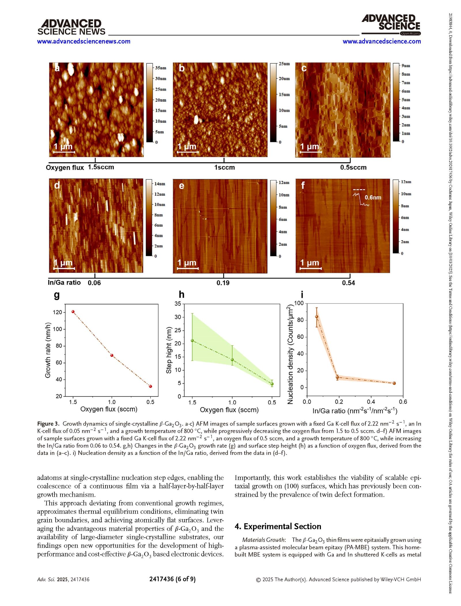
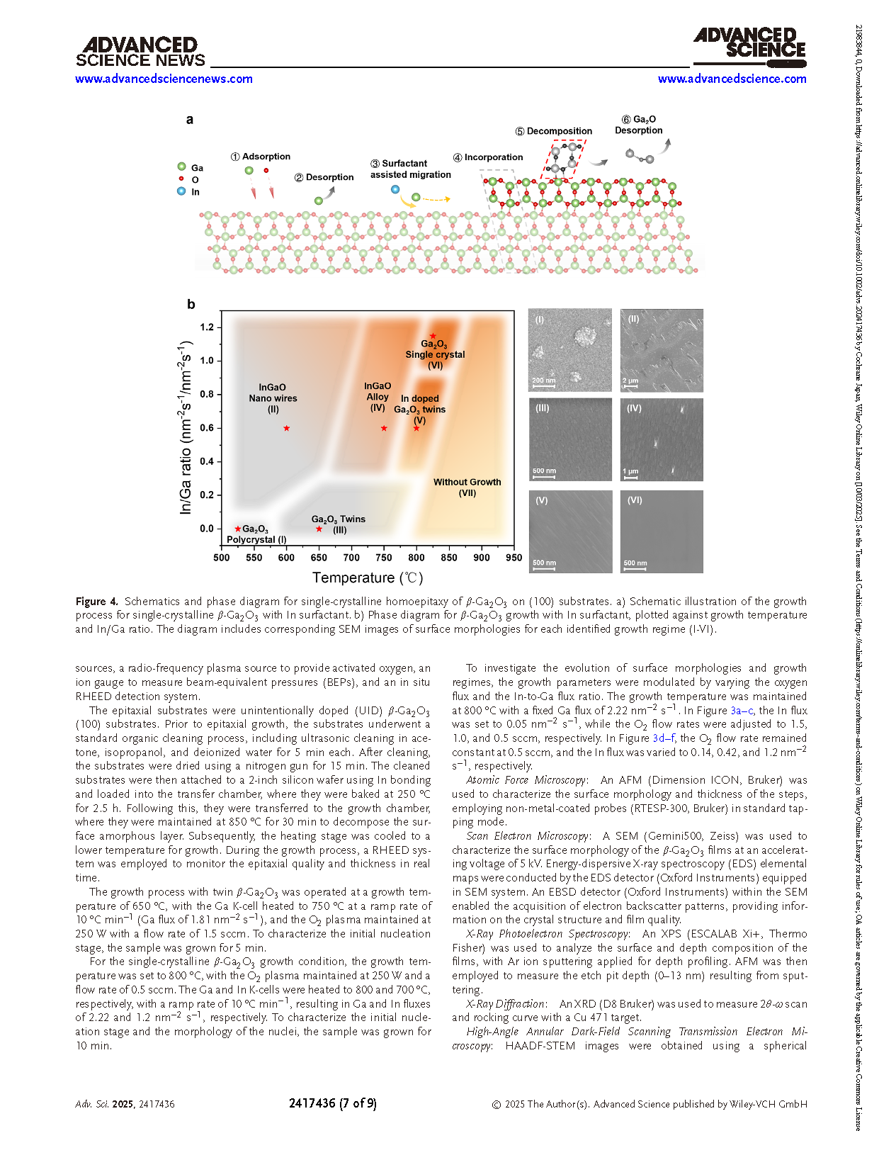
In this study, we successfully demonstrated the homoepitaxial growth of single-crystalline β-Ga₂O₃ on an on-axis (100) substrate using a van der Waals epitaxial strategy, akin to approaches employed for single-crystalline 2D material growth. By optimizing growth conditions with elevated temperatures and a high Ga/O ratio, we established a growth regime that enabled single-oriented nucleation on step-free surfaces. The incorporation of a metallic In surfactant further enhanced Ga adatom mobility, increasing the diffusion constant by three orders of magnitude compared to conventional twins growth conditions. This enhancement facilitated the migration and incorporation of Ga adatoms at single-crystalline nucleation step edges, enabling the coalescence of a continuous film via a half-layer-by-half-layer growth mechanism.
This approach deviating from conventional growth regimes, approximates thermal equilibrium conditions, eliminating twin grain boundaries, and achieving atomically flat surfaces. Leveraging the advantageous material properties of β-Ga₂O₃ and the availability of large-diameter single-crystalline substrates, our findings open new opportunities for the development of high-performance and cost-effective β-Ga₂O₃ based electronic devices. Importantly, this work establishes the viability of scalable epitaxial growth on (100) surfaces, which has previously been constrained by the prevalence of twin defect formation.
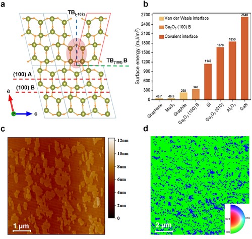
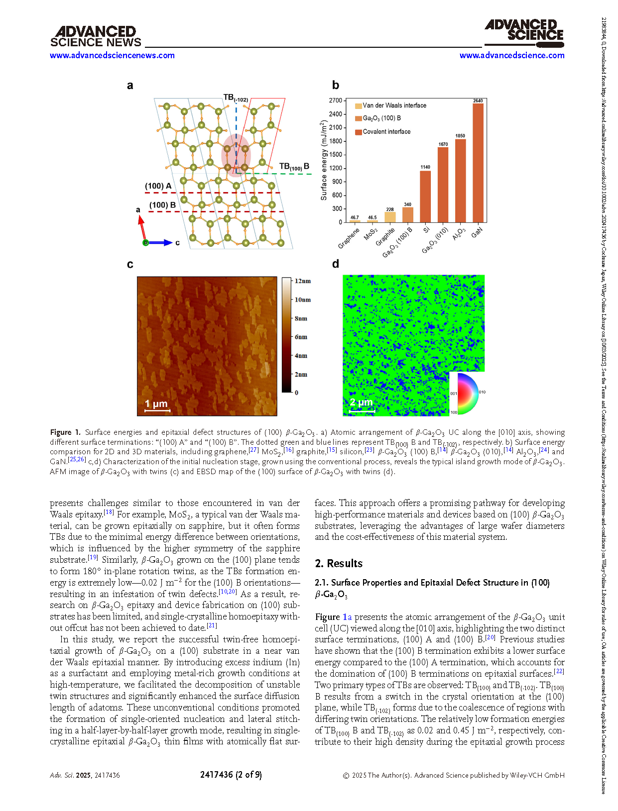
Figure 1. Surface energies and epitaxial defect structures of (100) β-Ga2O3. a) Atomic arrangement of β-Ga2O3 UC along the [010] axis, showing different surface terminations: “(100) A” and “(100) B”. The dotted green and blue lines represent TB(100) B and TB(-102), respectively. b) Surface energy comparison for 2D and 3D materials, including graphene, MoS2, graphite, silicon, β-Ga2O3 (100) B, β-Ga2O3 (010), Al2O3, and GaN. c,d) Characterization of the initial nucleation stage, grown using the conventional process, reveals the typical island growth mode of β-Ga2O3. AFM image of β-Ga2O3 with twins (c) and EBSD map of the (100) surface of β-Ga2O3 with twins (d).
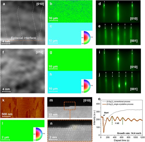
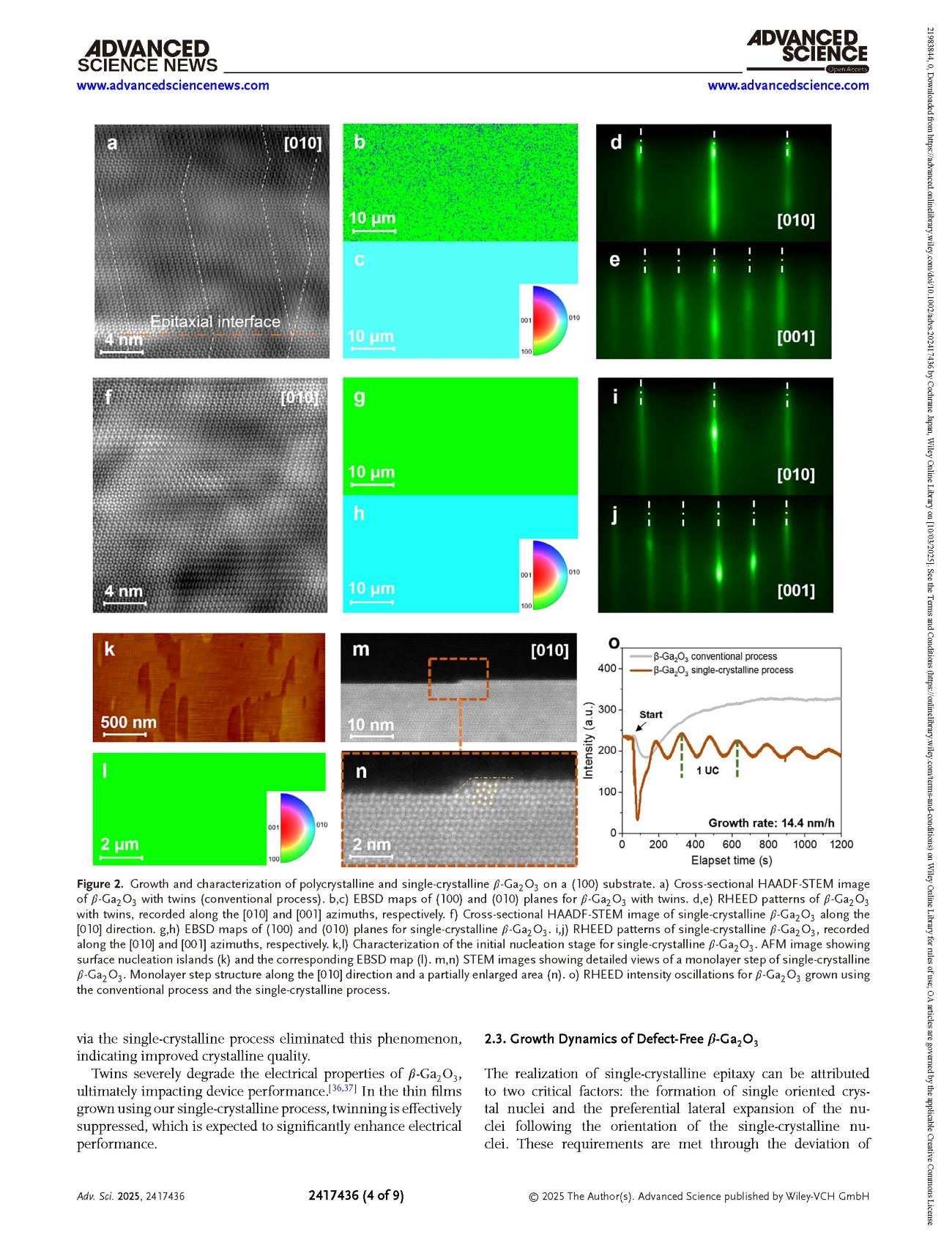
Figure 2. Growth and characterization of polycrystalline and single-crystalline β-Ga₂O₃ on a (100) substrate. a) Cross-sectional HAADF-STEM image of β-Ga₂O₃ with twins (conventional process). b,c) EBSD maps of (100) and (010) planes for β-Ga₂O₃ with twins. d,e) RHEED patterns of β-Ga₂O₃ with twins, recorded along the [010] and [001] azimuths, respectively. f) Cross-sectional HAADF-STEM image of single-crystalline β-Ga₂O₃ along the [010] direction. g,h) EBSD maps of (100) and (010) planes for single-crystalline β-Ga₂O₃. i,j) RHEED patterns of single-crystalline β-Ga₂O₃, recorded along the [010] and [001] azimuths, respectively. k,l) Characterization of the initial nucleation stage for single-crystalline β-Ga₂O₃. AFM image showing surface nucleation islands (k) and the corresponding EBSD map (l). m,n) STEM images showing detailed views of a monolayer step of single-crystalline β-Ga₂O₃. Monolayer step structure along the [010] direction and a partially enlarged area (n). o) RHEED intensity oscillations for β-Ga₂O₃ grown using the conventional process and the single-crystalline process.
DOI:
doi.org/10.1002/advs.202417436