Paper Sharing
【Member Papers】Xidian University —— 3 kV fully vertical β-Ga₂O₃ junction termination extension Schottky barrier diode with sputtered p-GaN
日期:2025-03-13阅读:903
Researchers from the Xidian University have published a dissertation titled "3 kV fully vertical β-Ga2O3 junction termination extension Schottky barrier diode with sputtered p-GaN" in Applied Physics Letters.
Program Support
This work was supported by the National Natural Science Foundation of China (Grant Nos. 62474135, 62104184, 62234009, 62090014, and 62404165), the China National Postdoctoral Program for Innovative Talents (Grant No. BX20200262), the China Postdoctoral Science Foundation (Grant Nos. 2021M692499 and 2023M732730), the Postdoctoral Fellowship Program of CPSF under Grant No. GZB20230557, the Natural Science Basic Research Program of Shaanxi under Grant (Program No. 2024JC-YBQN-0611).
Abstract
In this work, we present the fabrication of a fully vertical β-Ga2O3 Schottky barrier diode with junction termination extension (JTE-SBD) utilizing a p-GaN layer produced by sputtering, offering a solution to the absence of p-Ga2O3 materials. The p-GaN/n-Ga2O3 JTE-SBD demonstrates a turn-on voltage (Von) of 0.8 V, a specific on-resistance (Ron,sp) of 6.15 mΩ·cm2, an ideality factor (n) of 1.24, a breakdown voltage of 3 kV, and a Baliga's Figure of Merit of 1.46 GW/cm2. The current–voltage–temperature (I–V–T) testing has confirmed a transition in the dominant leakage mechanisms from the Poole–Frenkel mechanism to variable-range hopping.
Summary
In this study, we propose the fabrication of fully vertical p-GaN/ n-Ga2O3 JTE-SBD utilizing sputtered p-GaN. The JTE-SBD achieved a BV of 3kV with a BFOM of 1.46GW/cm2. I–V–T testing was con ducted to analyze the leakage current transport mechanisms for the JTE-SBD. It was found that PF is the dominant mechanism from 1 to 20V, with an emission barrier q/t of 0.74eV. VRH becomes dominant from 20 to 200V.
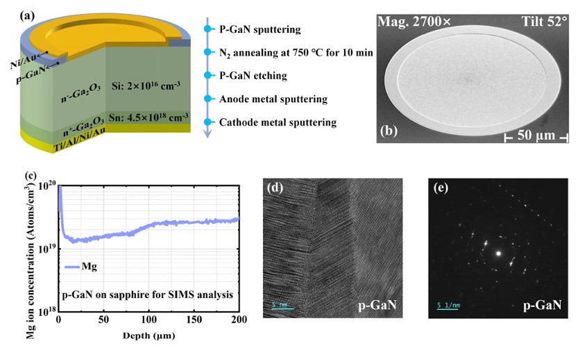
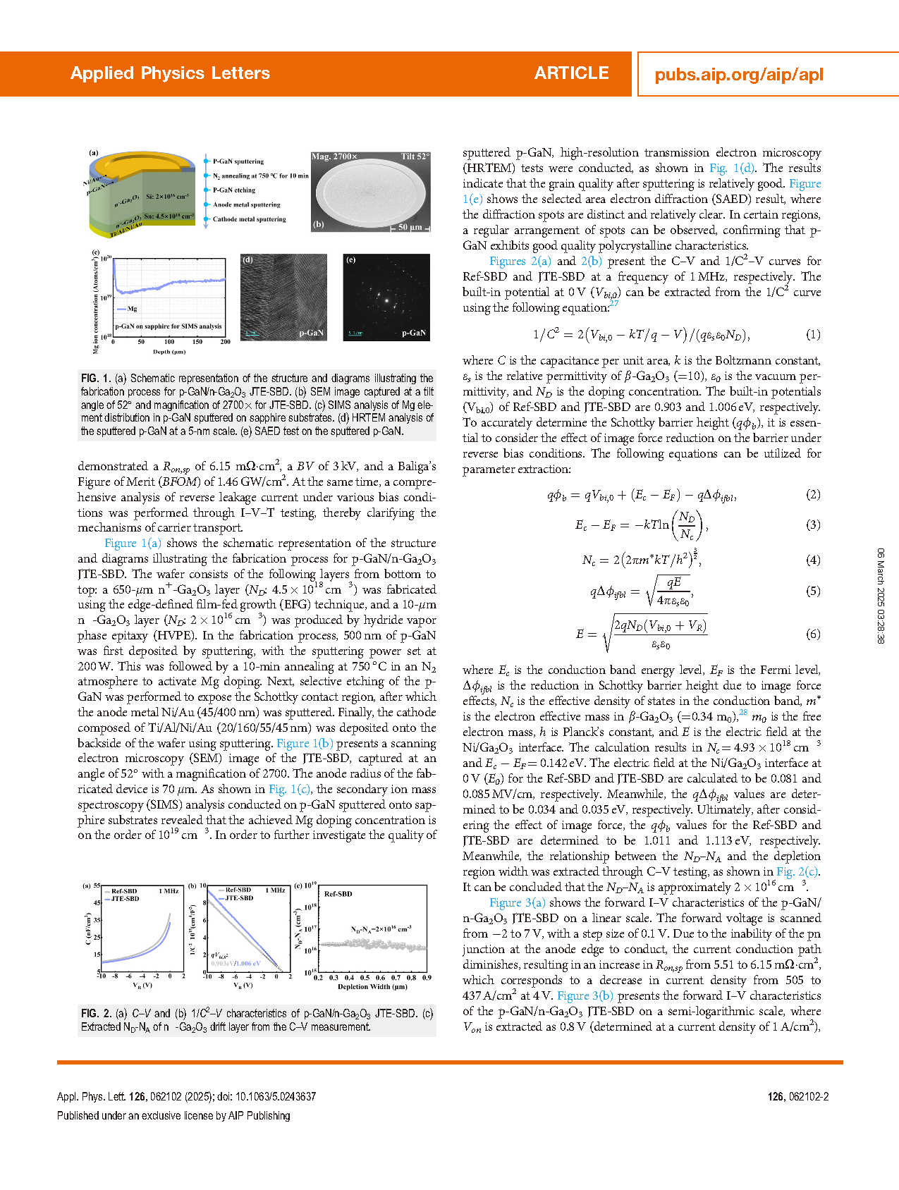
FIG. 1. (a) Schematic representation of the structure and diagrams illustrating the fabrication process for p-GaN/n-Ga2O3 JTE-SBD. (b) SEM image captured at a tilt angle of 52° and magnification of 2700 for JTE-SBD. (c) SIMS analysis of Mg ele ment distribution in p-GaN sputtered on sapphire substrates. (d) HRTEM analysis of the sputtered p-GaN at a 5-nm scale. (e) SAED test on the sputtered p-GaN.
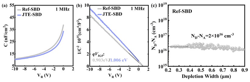
FIG. 2. (a) C–V and (b) 1/C2–V characteristics of p-GaN/n-Ga2O3 JTE-SBD. (c) Extracted ND-NA of n--Ga2O3 drift layer from the C–V measurement.
DOI:
doi.org/10.1063/5.0243637