Paper Sharing
【International Papers】Dielectric reliability and interface trap characterization in MOCVD grown in situ Al₂O₃ on β-Ga₂O₃
日期:2025-03-17阅读:775
Researchers from the University of California Santa Barbara have published a dissertation titled "Dielectric reliability and interface trap characterization in MOCVD grown in situ Al2O3 on β-Ga2O3" in Applied Physics Letters.
Corresponding Author Introduction

Sriram Krishnamoorthy
Ph.D. in Electrical Engineering, The Ohio State University
M.Sc. (Hons) in Physics, Birla Institute of Technology & Science (BITS)-Pilani
B.E. (Hons.) in Electrical and Electronics Engineering, Birla Institute of Technology & Science (BITS)- Pilani.
Prof. Krishnamoorthy's group works at the intersection of materials, electrical engineering and physics to study and engineer next-generation (ultra)wide band gap semiconductors such as Gallium Oxide. We are interested in epitaxial growth, electronic transport, design/modeling, micro/nano fabrication, and characterization of electronic/optoelectronic devices for a wide range of applications such as power electronics, high frequency electronics and ultra-violet optoelectronics.
Abstract
In this article, we investigate the in situ growth of Al2O3 on β-Ga2O3 using metal-organic chemical vapor deposition at a high temperature of 800 °C. The Al2O3 is grown within the same reactor as the β-Ga2O3, employing trimethylaluminum and O2 as precursors without breaking the vacuum. We characterize the shallow and deep-level traps through stressed capacitance–voltage (C–V) and photo-assisted C–V methods. The high-temperature deposited dielectric demonstrates an impressive catastrophic breakdown field of approximately 10 MV/cm. Furthermore, we evaluate the reliability and lifetime of the dielectrics using time-dependent dielectric breakdown measurements. By modifying the dielectric deposition process to include a high-temperature (800 °C) thin interfacial layer and a low-temperature (600 °C) bulk layer, we report a 10-year lifetime under a stress field of 3.5 MV/cm along a catastrophic breakdown field of 7.8 MV/cm.
Summary
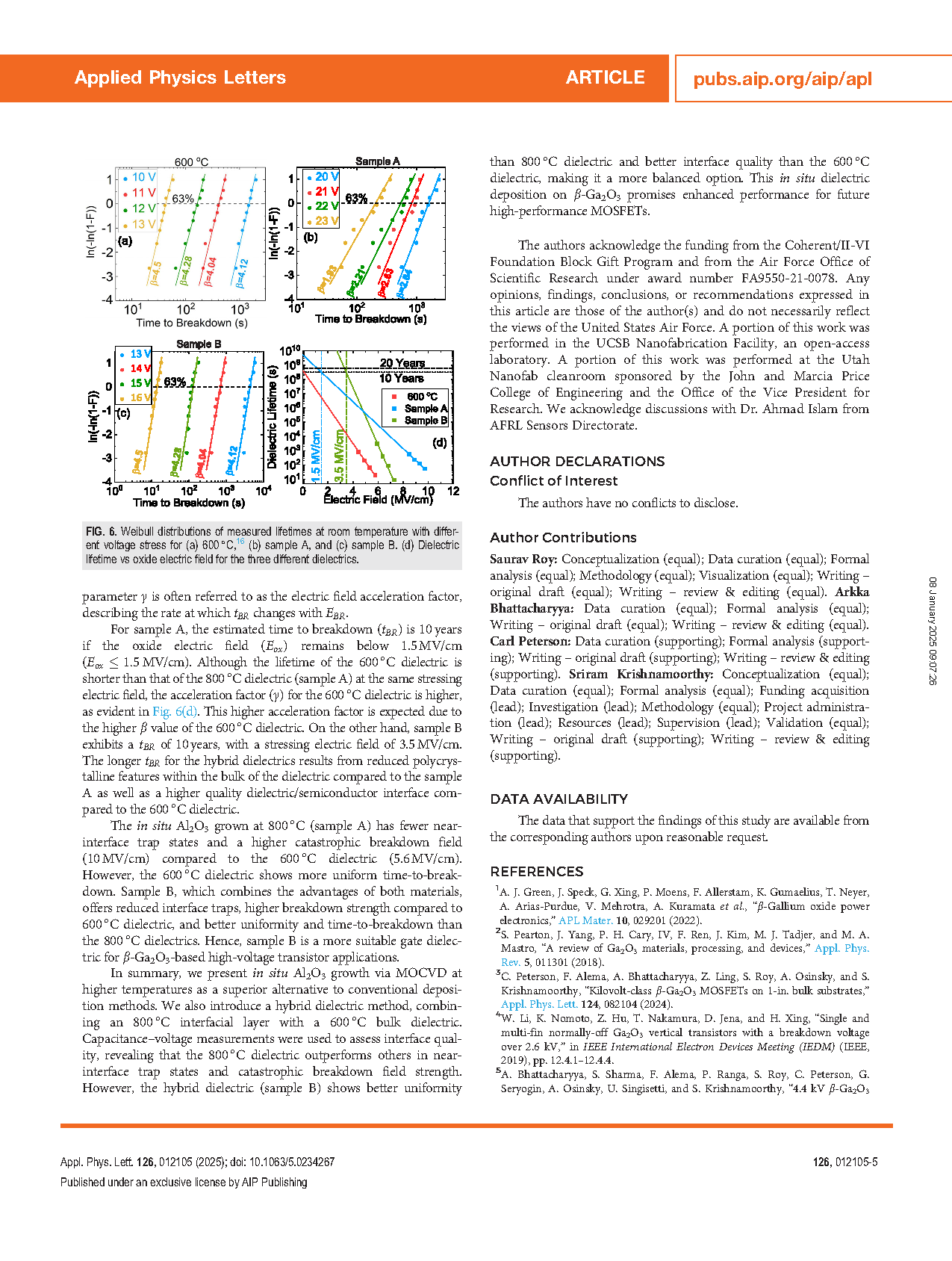
In summary, we present in situ Al2O3 growth via MOCVD at higher temperatures as a superior alternative to conventional deposition methods. We also introduce a hybrid dielectric method, combining an 800°C interfacial layer with a 600°C bulk dielectric. Capacitance–voltage measurements were used to assess interface quality, revealing that the 800°C dielectric outperforms others in near interface trap states and catastrophic breakdown field strength. However, the hybrid dielectric (sample B) shows better uniformity than 800°C dielectric and better interface quality than the 600°C dielectric, making it a more balanced option. This in situ dielectric deposition on β-Ga2O3 promises enhanced performance for future high-performance MOSFETs.
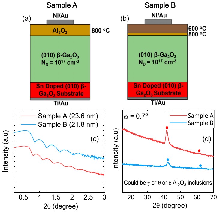
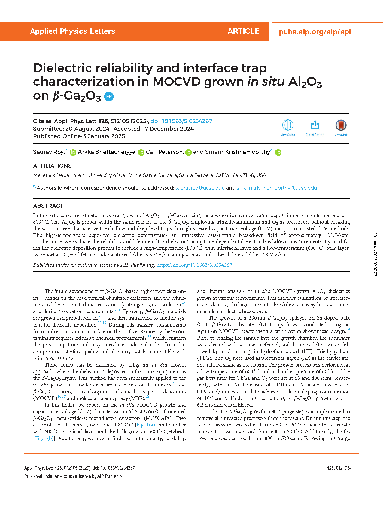
FIG. 1. Schematic diagram of the fabricated MOSCAP structures with (a) sample A (800 °C) and (b) sample B (800/600 °C). (c) X-ray reflectivity plot and (d) GIXRD spectra for sample A and sample B.
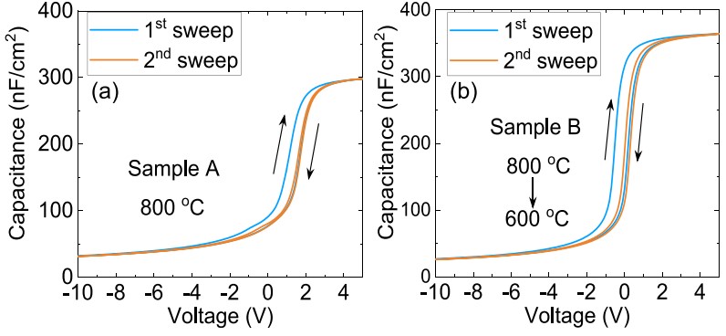
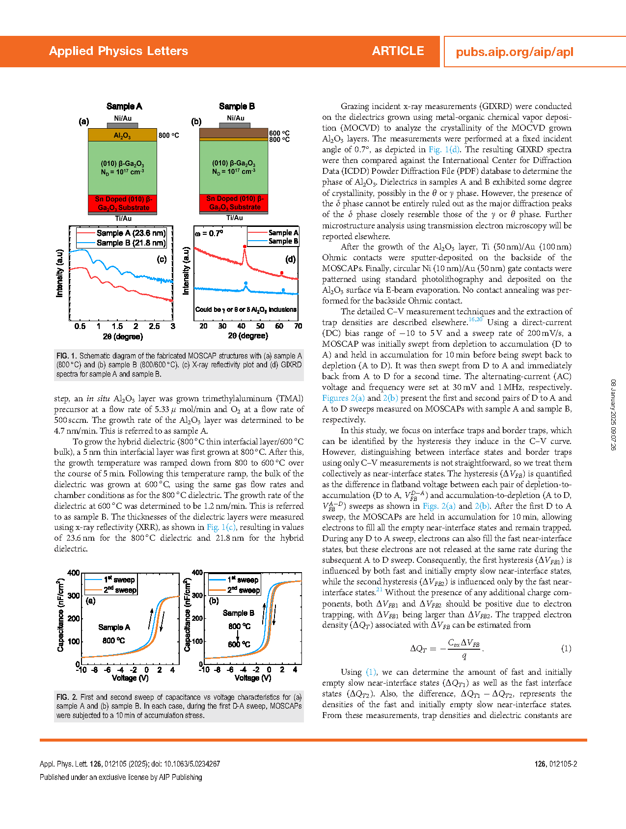
FIG. 2. First and second sweep of capacitance vs voltage characteristics for (a) sample A and (b) sample B. In each case, during the first D-A sweep, MOSCAPs were subjected to a 10 min of accumulation stress.
DOI:
doi.org/10.1063/5.0234267