Paper Sharing
【Member Papers】Researchers from the JFS Laboratory of Interface states in semiconductor and their influence on Schottky barrier in β-Ga₂O₃
日期:2025-03-18阅读:852
Researchers from the JFS Laboratory have published a dissertation titled " Interface states in semiconductor and their influence on Schottky barrier in β-Ga2O3" in Surfaces and Interfaces.
Acknowledgments
This work was supported by the Major Program (JD) of Hubei Province under Grant No. 2023BAA009.
Background
β-Ga2O3 is a promising candidate for power electronics, solar blind detectors, and sensors with capabilities beyond exiting techniques due to its ultra-high band gap which gives rise to the higher power and lower on-resistance, cheaper substrates that can be fabricated via standard melt-growth techniques, and well suitable fabrication processing. The techniques involving in improving performance of β-Ga2O3 devices have been extensively investigated, including heteroepitaxial growth of p type materials, hetero-bonding for heat transportation, and fabrication of heterostructure FETs (Field Effect Transistor) for higher electronic mobility. Because of its high breakdown electric field, β-Ga2O3 based Schottky Barrier Diode (SBD) shows higher power figure of merit and more practical advantages over other materials based devices which need more complicated structures to achieve the similar performance. β-Ga2O3 SBD is now undergoing transition from laboratory to commercialization.
Abstract
The density of surface and interface states versus Schottky barrier in β-Ga2O3 has been numerically calculated by taking into account of neutrality level, work function, intermediate insulator thickness, and dopant concentration. It was found there exists a critical neutrality level at which interfacial state has the minimum effects on the Schottky barrier. Comparison with experimental observations shows Ohmic contact exhibits a lower neutrality level resulting in the rise of Schottky barrier and Schottky contact has a higher neutrality level leading to the drop of Schottky barrier. The findings indicate Ohmic contact or Schottky contact can be improved if more acceptor type defects or more donor type defects are generated on the interface after treatment respectively.
Summary
The effect of interface trap density on Schottky barrier in β-Ga2O3 in terms of work function, neutrality level, intermediate insulator thickness, and dopant concentration has been investigated by numerical simulation of Poisson’s equation assuming interface traps have donor or acceptor type behavior satisfying the Fermi’s occupation statistics. Depending on neutrality level, interface states can either enhance or weaken the Schottky barrier. A critical neutrality level was found at Eg − eΦ0 = eΦm − ex where interface traps have minimum effects on the Schottky barrier. Since low work function metals are used in Ohmic contact and almost all neutrality levels satisfy Eg − eΦ0 > eΦm −ex, Schottky barrier are always larger than expected value. For Schottky contact, a high neutrality level was found and Eg− eΦ0 < eΦm − ex is satisfied, giving lower Schottky barrier than expected. Regarding surface treatments, more donor type defects generated on the surface, giving downward band bending, are beneficial to Ohmic contact, and more acceptor type defects on the surface, on the contrary, giving upward band bending, are desired for Schottky contact. These findings are well consistent with experimental observations and surface treatments. In addition, no correlation between dangling bonds and Schottky barrier can be identified. And more, two neutrality levels were found by comparison with experimental observations, one of which has been reported.
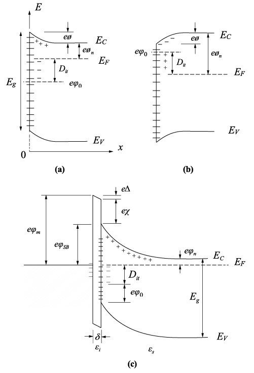
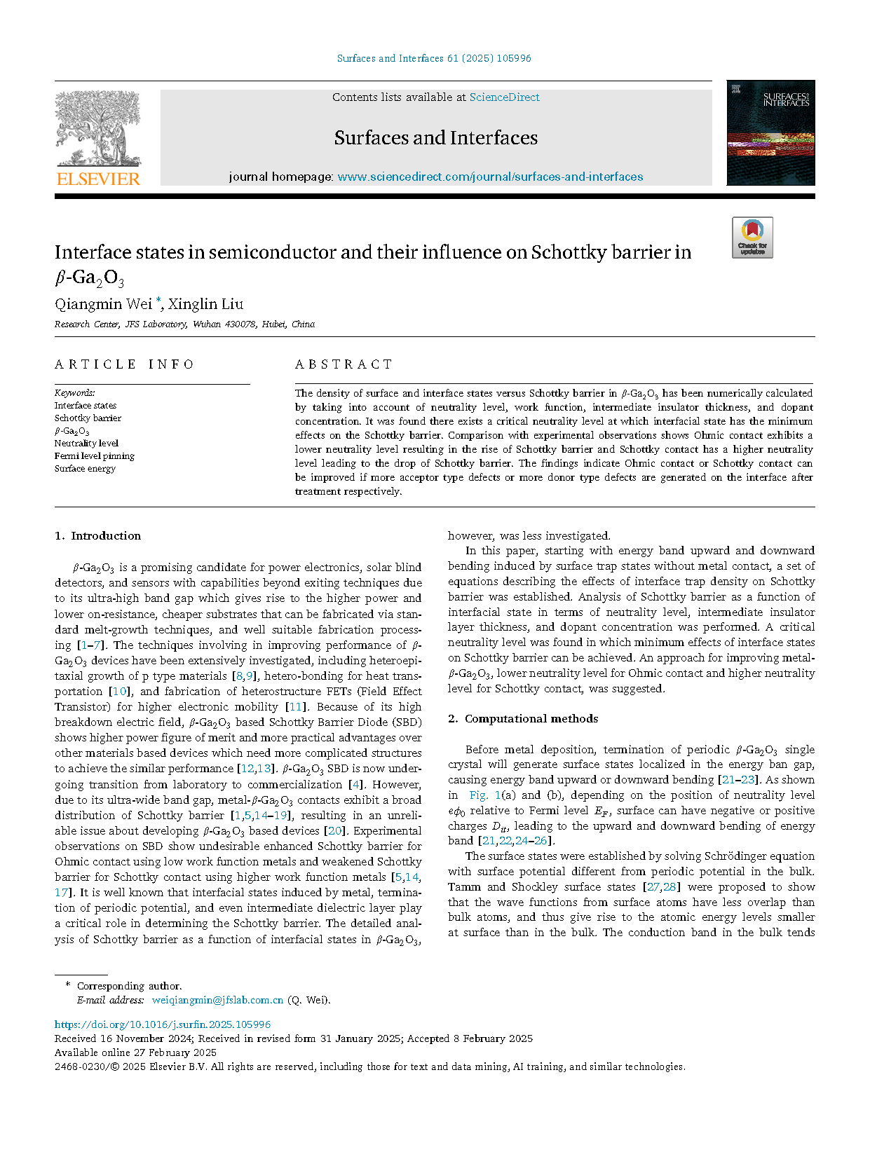
Fig. 1. Schematic representation of band diagram with surface states under thermal equilibrium. (a) Upward and (b) downward band bending induced by surface states without metal deposition. (c) Relationship between interfacial trap density and Schottky barrier in terms of metal work function, semiconductor affinity, and intermediate dielectric layer.
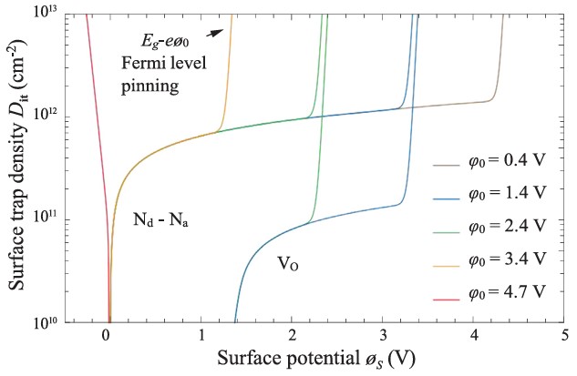
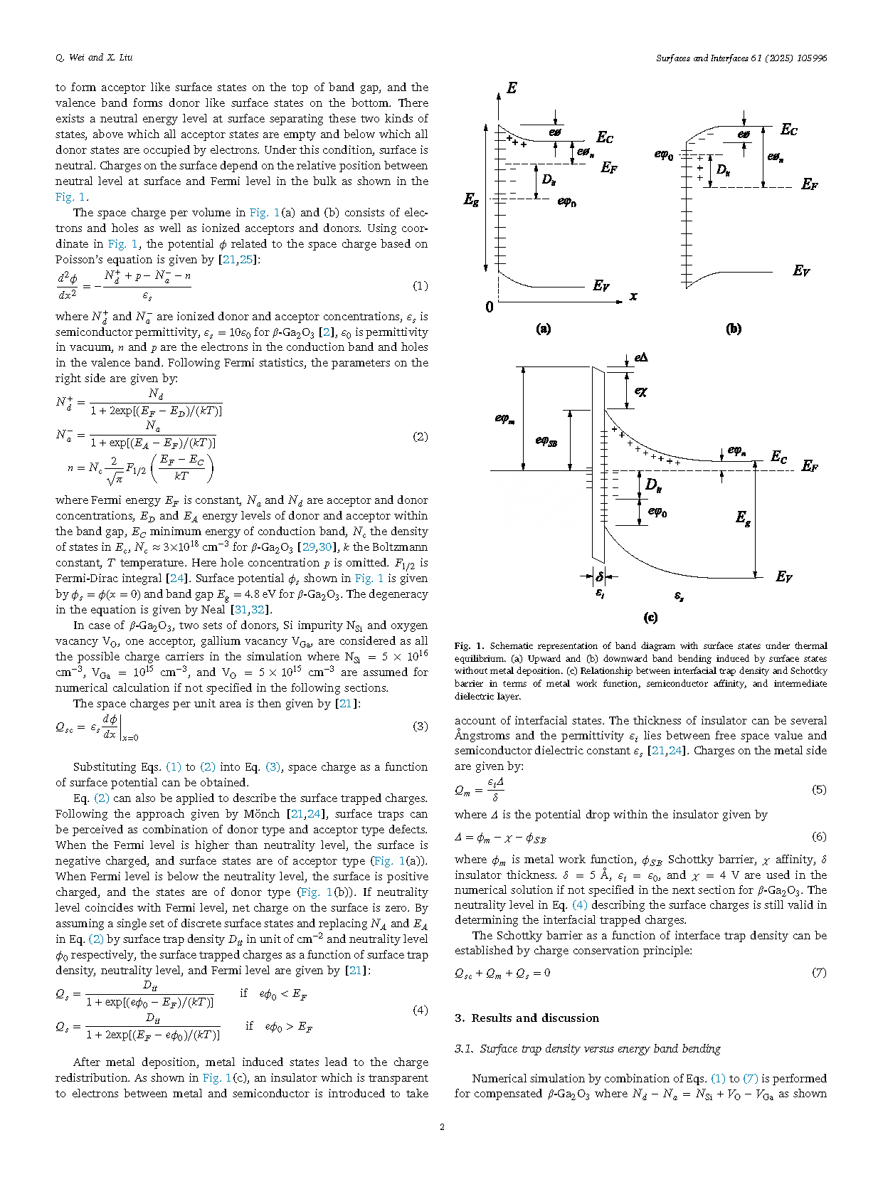
Fig. 2. Numerical simulation representing the surface band bending as a function of surface trap density in β-Ga2O3 in terms of neutrality levels, net concentration Nd-Na, and oxygen vacancy Vo.
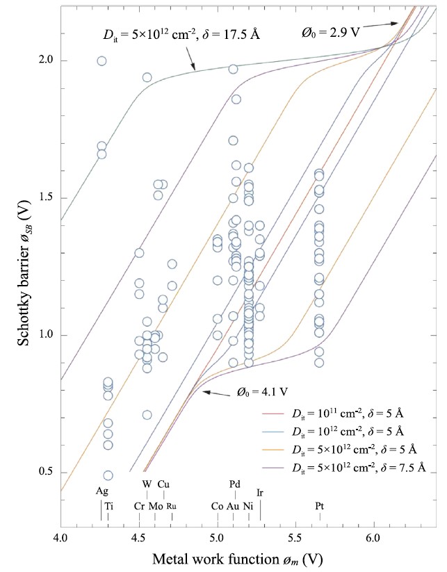
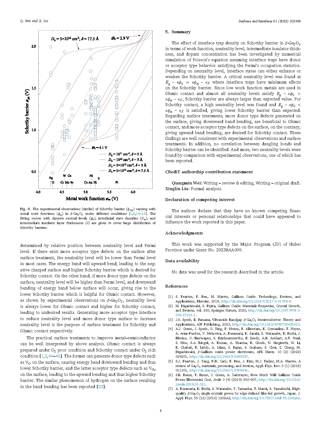
Figure 3: The experimental observations (circles) of Schottky barrier (ϕSB) varying with metal work functions (ϕm) in β-Ga2O3 under different conditions. The fitting curves with discrete neutral levels (ϕ0), interfacial state densities (Dit), and intermediate insulator layer thicknesses (δ) are given to cover large distribution of Schottky barriers.
DOI:
doi.org/10.1016/j.surfin.2025.105996