Paper Sharing
【Domestic Papers】 University of Science and Technology of China --- Improvement of interface quality through low-temperature annealing in β-Ga₂O₃ diode with compounded mesa and junction termination extension
日期:2025-03-18阅读:771
Researchers from the University of Science and Technology of China have published a dissertation titled "Improvement of interface quality through low-temperature annealing in β-Ga2O3 diode with compounded mesa and junction termination extension" in Applied Physics Letters.
Program Support
This work was supported by the National Natural Science Foundation of China (Grant Nos. U23A20358, 62234007, 62474170, 62404214, and 61925110), the National Key Research and Development Program of China (No. 2024YFE0205200), the JieBang Headed Project of Changsha City Hunan Province (Grant No. kq2301006), and the Opening Project of and the Key Laboratory of Nanodevices and Applications in Suzhou Institute of Nano-Tech and Nano-Bionics of CAS. This work was partially carried out at the Center for Micro and Nanoscale Research and Fabrication, the Information Science Laboratory Center, and the Instruments Center for Physical Science of USTC.
Background
β-Ga2O3 has been emerging as a promising material for high voltage and high-power applications due to its ultra-wide bandgap (4.5–4.9 eV), high critical electrical field (8 MV/cm), and cost-effective single crystal melt growth. In the past decade, β-Ga2O3 unipolar devices have undergone significant development using field plates, ion implantation, p-type NiO (p-NiO) based junction termination extension (JTE) or guard rings, as well as trench and mesa techniques. Among these termination techniques, mesa technique has shown significant effectiveness in electric field management as a stand-alone termination in devices. A record plate electric field exceeding 4.1MV/cm has been achieved by mesa termination design in β-Ga2O3 Schottky barrier diodes (SBDs). Although the mesa termination can significantly reduce the surface electric field, the peak electric field moves from the edge of the anode to the mesa sidewall and corner. Therefore, it is necessary to alleviate the concentration of electric field exerted at the mesa termination. An oxide dielectric field plate was proposed to expand the electric field concentration at the mesa sidewall and corner.
Abstract
The ultra-wide bandgap semiconductor β-Ga2O3 has facilitated the development of Schottky barrier diodes with high breakdown voltage and low power losses. Designing effective termination structures is a critical step in exploiting the advantages of β-Ga2O3 power diodes. Among various types of termination structures, mesa technique features a simple preparation process and theoretically high efficiency electric field management capability in β-Ga2O3 devices. In order to further reduce the peak electric field along the mesa sidewall and corner, the p-type NiO junction termination extension (JTE) structure was incorporated. However, deep level transient spectroscopy revealed a new shallow energy level at Ec–0.28 eV related to interface states inducing by dry etching, which is the cause of the weakened JTE structure effect and instability of electrical properties. A low-temperature post-annealing process was proposed to eliminate the interface states, thereby achieving better charge balance and enhancing the breakdown voltage of compounded termination device from 1.35 to 2.1 kV without sacrificing the forward characteristics. This work reveals the energy level related to interface states introduced by dry etching in β-Ga2O3 and facilitates the fabrication of high-performance devices.
Graphical Abstract
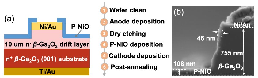
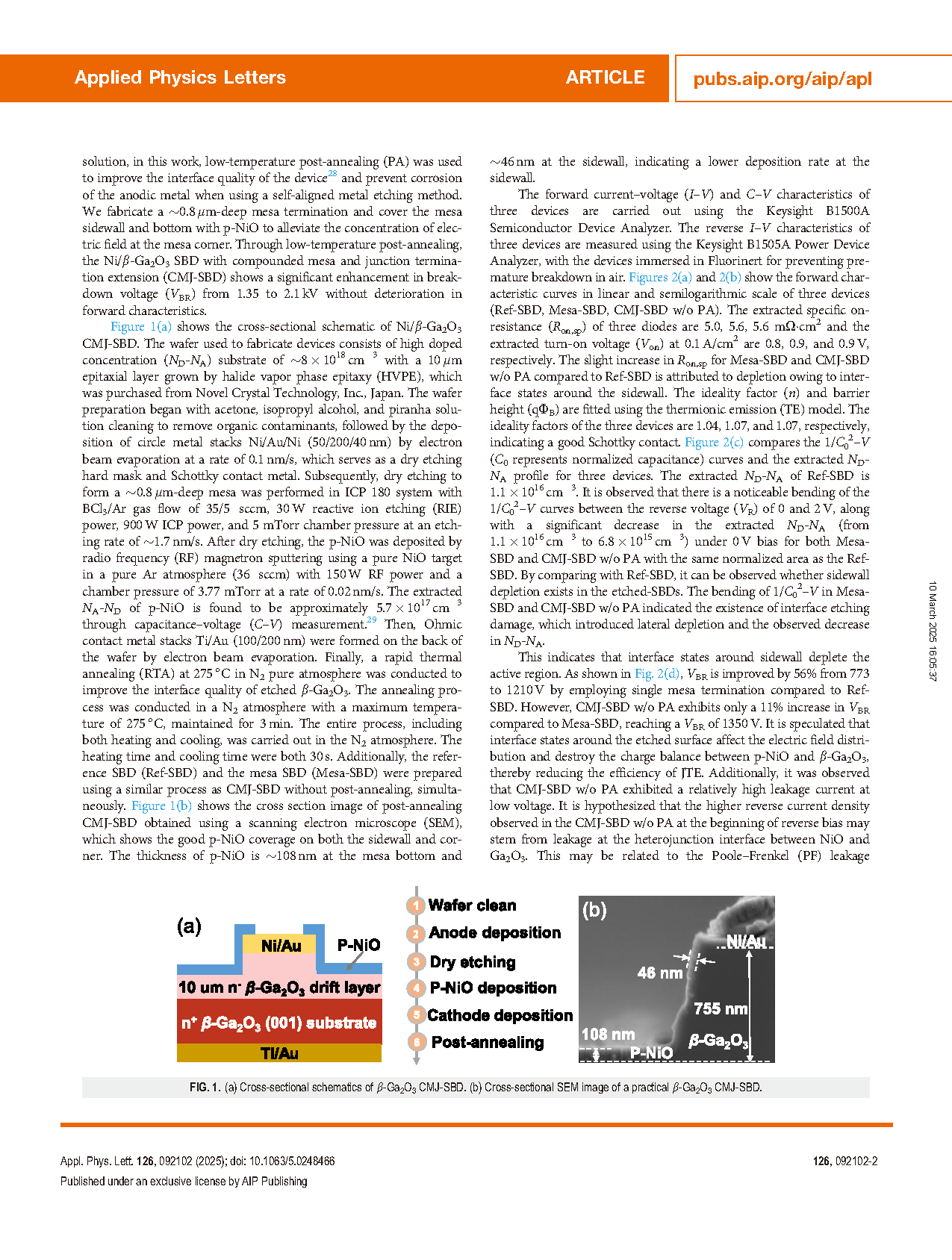
FIG. 1. (a) Cross-sectional schematics of β-Ga2O3 CMJ-SBD. (b) Cross-sectional SEM image of a practical β-Ga2O3 CMJ-SBD.
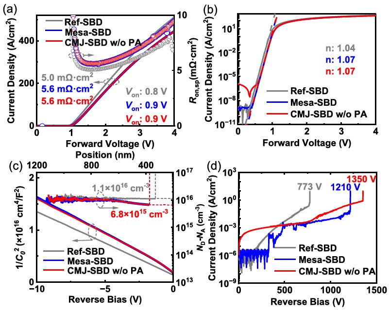
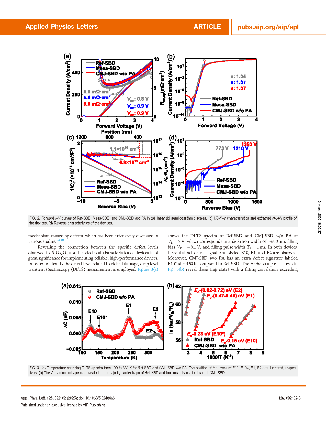
FIG. 2. Forward I–V curves of Ref-SBD, Mesa-SBD, and CMJ-SBD w/o PA in (a) linear (b) semilogarithmic scales. (c) 1/C02–V characteristics and extracted ND-NA profile of the devices. (d) Reverse characteristics of the devices.
DOI:
doi.org/10.1063/5.0248466