


Paper Sharing
【Device Papers】The characteristics of line-shaped defects and their impact mechanism on device performance in β-Ga₂O₃ Schottky barrier diode
日期:2025-03-20阅读:807
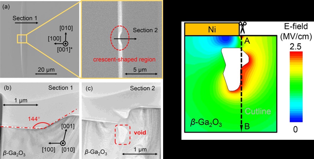
The defect of crystal is a major factor affecting the performance and life of semiconductor devices. For β-Ga2O3, which has great application potential in the field of high power devices, it is very important to study the relationship between defect of crystal and device performance. Recently, a research team led by Professor Shibing Long and Guangwei Xu of the University of Science and Technology of China (USTC) used emission microscopy, transmission electron microscopy and atomic force microscopy to investigate the characteristics, formation and effects of linear defects in Halide Vapor Phase Epitaxial (HVPE) Si doped (001) β-Ga2O3 Schottky Barrier Diode (SBD). It is found that the linear defect from the void is the main reason for the increase of leakage current and premature breakdown of SBD. This study illustrates the effect of linear defect on the device performance, which is of great significance for improving the performance of β-Ga2O3 devices. Relevant research results are presented in " The characteristics of line-shaped defects and their impact mechanism on device performance in β-Ga2O3 Schottky barrier diodes "is published in Applied Physics Letters.
Abstract:
Beta-phase Gallium Oxide (β-Ga2O3) has attracted increasing attention in the field of power electronic devices due to its ultra-wide bandgap and high Baliga figure-of-merit. However, the premature breakdown deteriorated with the increase in device area, hindering the scale-up of the current rating. In this work, we unveil the formation and characteristics of killer defects responsible for the premature breakdown in an Si-doped (001) β-Ga2O3 epitaxial layer grown by halide vapor phase epitaxy. The killer defects feature a line-shaped morphology along the [010] orientation. Specifically, the high-resolution transmission electron microscopy characterization links the line-shaped defects to underlying voids. These voids are surrounded by amorphous phase regions, and the transition from amorphous phase to crystalline phase results in twins extending along the [010] orientation, which eventually become line-shaped defects on the wafer. Additionally, the defect area exhibits smaller capacitance and lower surface potential compared to the defect-free region. This is attributed to the absence of local ionized donors in the defect area, leading to electric field concentration in this region. This study systematically investigates a killer defect in β-Ga2O3, which contributes to the scale-up process of β-Ga2O3 power devices and advances their application.
DOI:
10.1063/5.0244107
