Paper Sharing
【Member Papers】 Researchers Led by Prof. Kelvin H. L. Zhang from the Xiamen University——Electronic structure and surface band bending of Sn-doped β-Ga₂O₃ thin films studied by x-ray photoemission spectroscopy and ab initio calculations
日期:2025-03-31阅读:790
Researchers from the Xiamen University have published a dissertation titled "Electronic structure and surface band bending of Sn-doped β-Ga2O3 thin films studied by x-ray photoemission spectroscopy and ab initio calculations" in Physical Review B.
Acknowledge
The authors acknowledge funding support from National Key R&D Program of China (Grant No. 2022YFB3605501) and National Natural Science Foundation of China (Grant No. 22275154). J.W. and D.S. acknowledge Diamond Light Source for cosponsorship of an EngD studentship on the EPSRC Centre for Doctoral Training in Molecular Modelling and Materials Science (EP/L015862/1). D.S. acknowledges support for EPSRC (Grant No. EP/N01572X/1). This work used the ARCHER and ARCHER2 UK National Supercomputing Service, via our membership in the UK’s HEC Materials Chemistry Consortium, which is funded by EPSRC (Grants No. EP/L000202, No. EP/R029431, and No. EP/T022213). We are grateful to the UK Materials and Molecular Modelling Hub for computational resources (Thomas and Young), which is partially funded by EPSRC (EP/P020194/1 and EP/T022213/1). The authors acknowledge the use of the UCL Myriad, Kathleen, and Thomas High Performance Computing Facilities (Myriad@UCL, Kathleen@UCL,Thomas@UCL),and associated support services, in the completion of this work. Work by P.M. and O.B. was performed in the framework of GraFOx, a Leibniz ScienceCampus partially funded by the Leibniz association. We are grateful to the Diamond Light Source for access to beamline I09 under Proposals No. SI31069 and No. SI31681.
Background
Monoclinic β-phase Ga2O3 has garnered significant interest as a wide band gap semiconductor for various device applications, including high-power electronics, solar-blind deep ultraviolet (DUV) photodetectors, and DUV transparent conductive oxides (TCOs). This is due to its ultralarge band gap of approximately 4.8 eV, high theoretical breakdown field of 8 MV/cm, controllable n-type dopability, and availability of large-scale substrate wafers grown from the melt. However, doping not only affects carrier transport properties but also introduces additional electronic states, which alter the electronic and optical characteristics of the material. Therefore, understanding the impact of n-type doping on the electronic structure of β-Ga2O3 is critical for device design.
Abstract
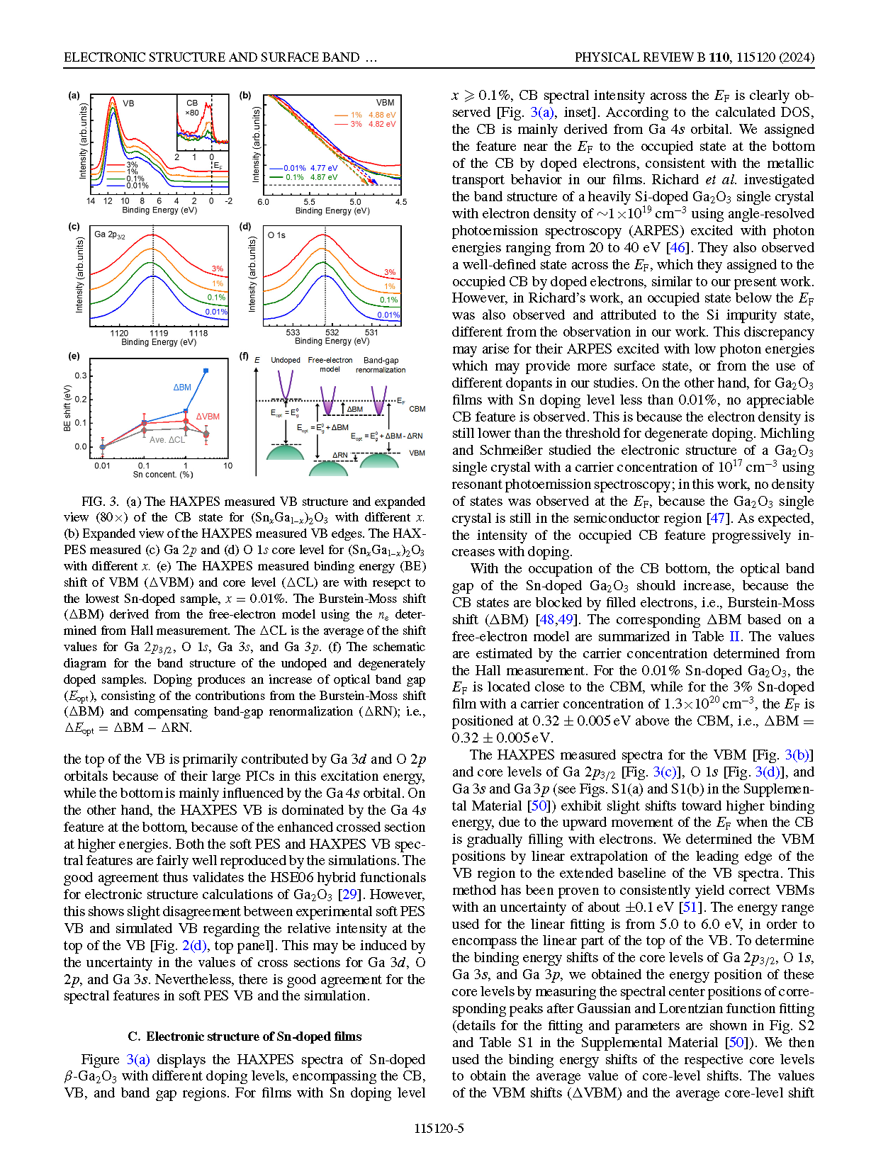
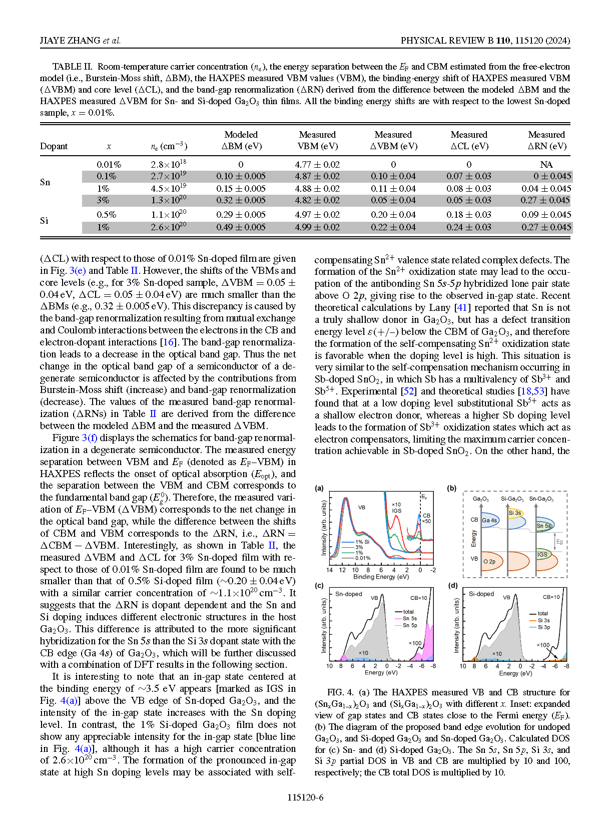
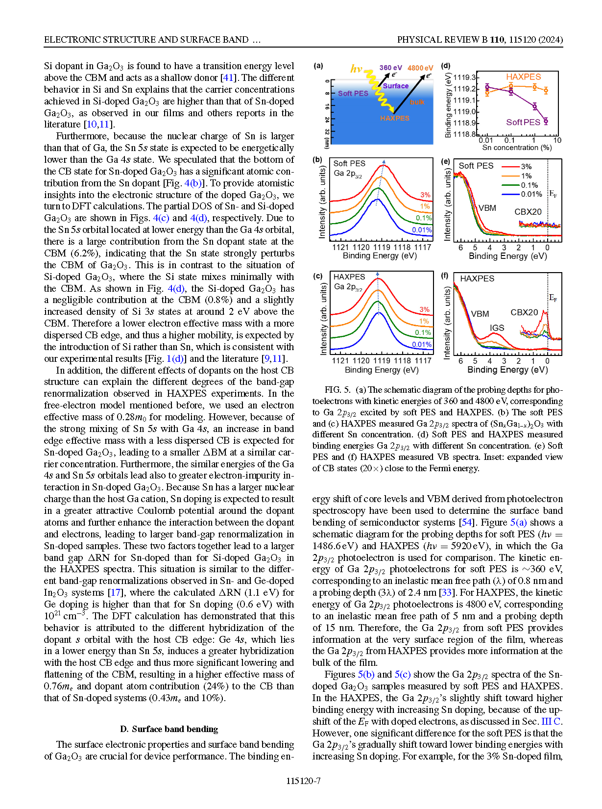
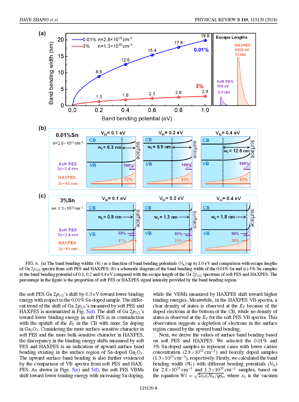
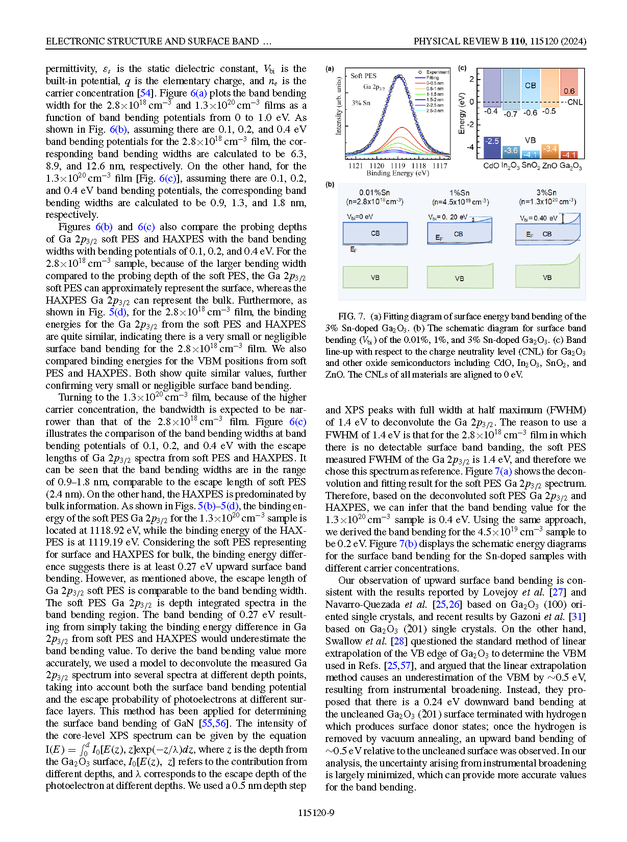
The bulk and surface electronic structures of Sn-doped β-Ga2O3 thin films have been studied by soft and hard x-ray photoemission spectroscopy (soft PES at 1486.6 eV and HAXPES at 5920 eV). The experimental spectra are compared with density functional theory calculated density of states in the valence band and conduction band. Excellent agreement was found between experimental spectra and calculated density of states by taking into account the photoionization cross section of different orbitals involved in the valence and conduction bands. The electronic states derived from Ga 4s character are selectively enhanced by HAXPES. This allows us to infer that the states at the conduction band and bottom of the valence band contain pronounced Ga 4s character. The occupation of the lower conduction band in degenerately Sn-doped Ga2O3 is clearly observed by HAXPES, which allows for direct measurement of Burstein-Moss shift and band-gap renormalization as a function of Sn doping. A comparison of the valence band spectra of Sn-doped Ga2O3 films with Si-doped samples suggests that Sn doping has different effects on the electronic structure than Si doping. An in-gap electronic state is observed for Sn-doped Ga2O3, which is attributed to self-compensating Sn2+ related defects. Furthermore, a larger band-gap renormalization is found in Sn-doped samples, because the Sn 5s dopant orbital mixes strongly with the host Ga 4s derived conduction band. Finally, a comparison of the valence band and core-level spectra excited with soft and hard x rays allows us to identify an upward band bending at the surface region of Sn-doped Ga2O3 films.
Conclusion
In summary, a combination of soft and hard x-ray photoemission spectroscopy and density functional theory has been used to study the bulk and surface electronic structures of Sn-doped Ga2O3 thin films. Excellent agreement was found between the experimental valence band spectra and calculated density of states for lightly doped Ga2O3 by taking into account the photoionization cross section of different orbitals. It has been found that the electronic states at the conduction band and bottom of the valence band are selectively enhanced in HAXPES relative to soft PES. This is attributed to the fact that these states have substantial Ga 4s character. With increasing Sn doping in Ga2O3, the occupation of the lower conduction band is clearly observed by HAXPES, which allows for the direct determination of band-gap renormalization as a function of Sn doping. Relatively larger band-gap renormalization was found in Sn-doped Ga2O3 films in com parison with Si-doped Ga2O3 samples, because the Sn 5s state mixes strongly with the host Ga 4s derived conduction band, as further proved by theoretical calculation. Furthermore, an in-gap state is observed for Sn-doped Ga2O3, which is attributed to self-compensating Sn2+ related defect states. Insights in electronic structures of Sn-doped Ga2O3 may ex plain the higher activation energy and lower electron mobility observed in Sn-doped Ga2O3 films in the literature. Finally, a comparison of the valence band and core-level spectra excited with soft and hard x rays allows us to identify the existing upward surface band bending in the Sn-doped Ga2O3.
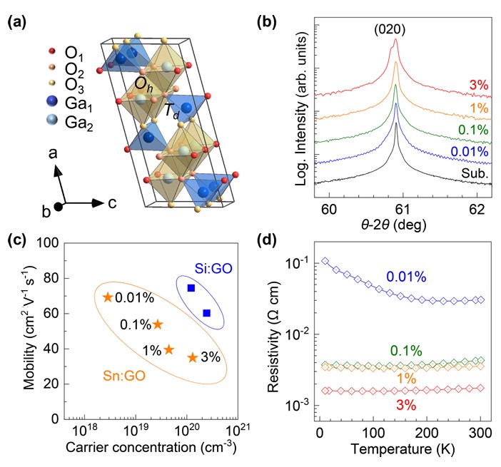
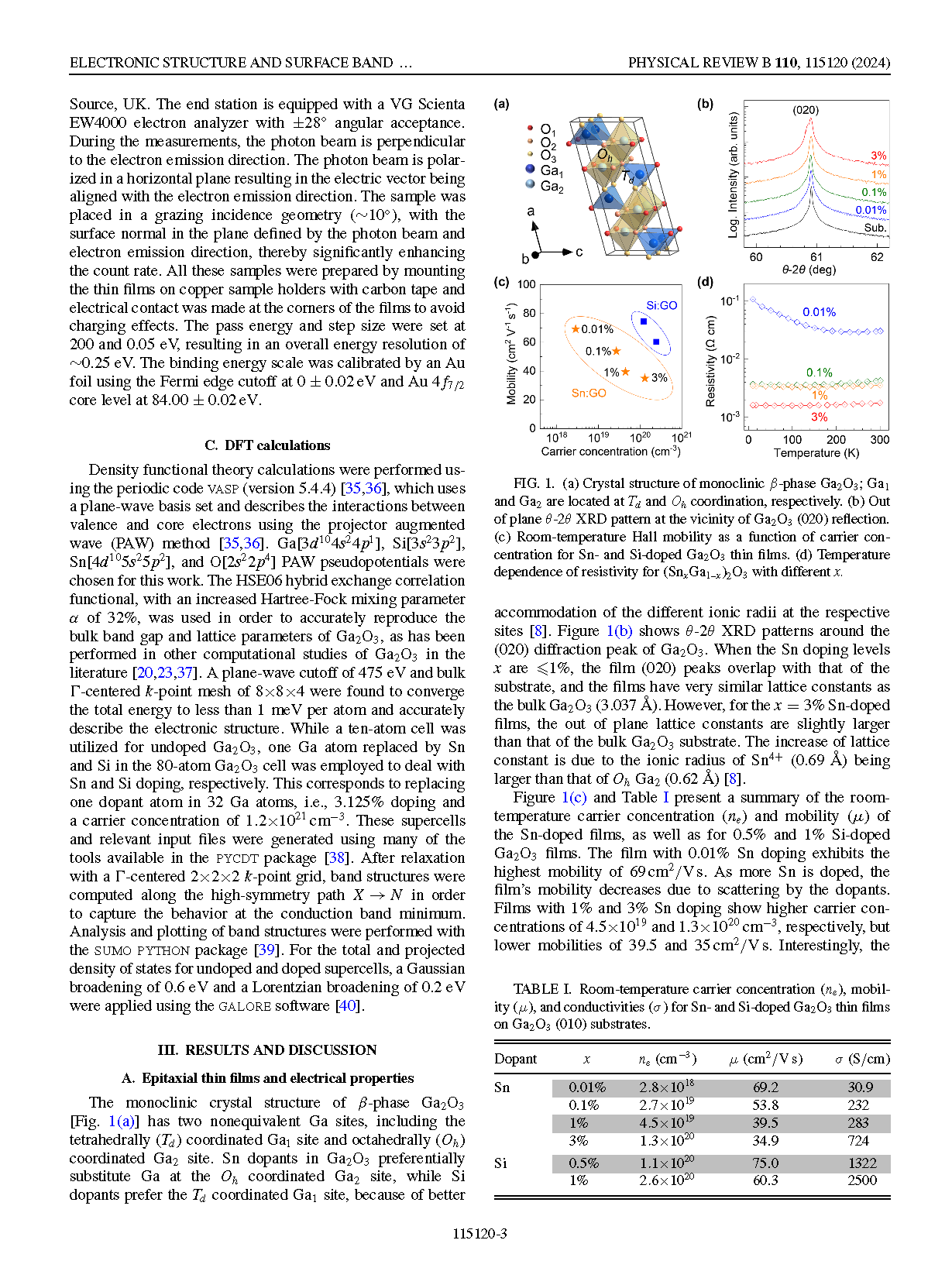
FIG.1. (a)Crystal structure of monoclinic β-phase Ga2O3; Ga1 and Ga2 are located at Td and Oh coordination, respectively. (b)Out of plane θ-2θ XRD pattern at the vicinity of Ga2O3(020) reflection. (c)Room-temperature Hall mobility as a function of carrier concentration for Sn- and Si-doped Ga2O3 thin films. (d)Temperature dependence of resistivity for (SnxGa1–x)2O3 with different x.
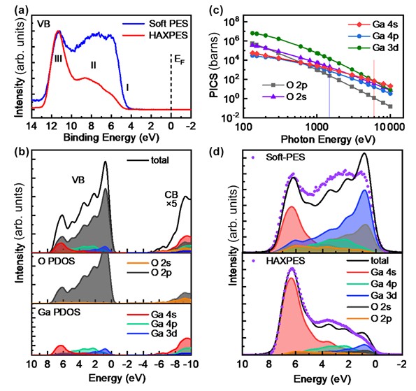
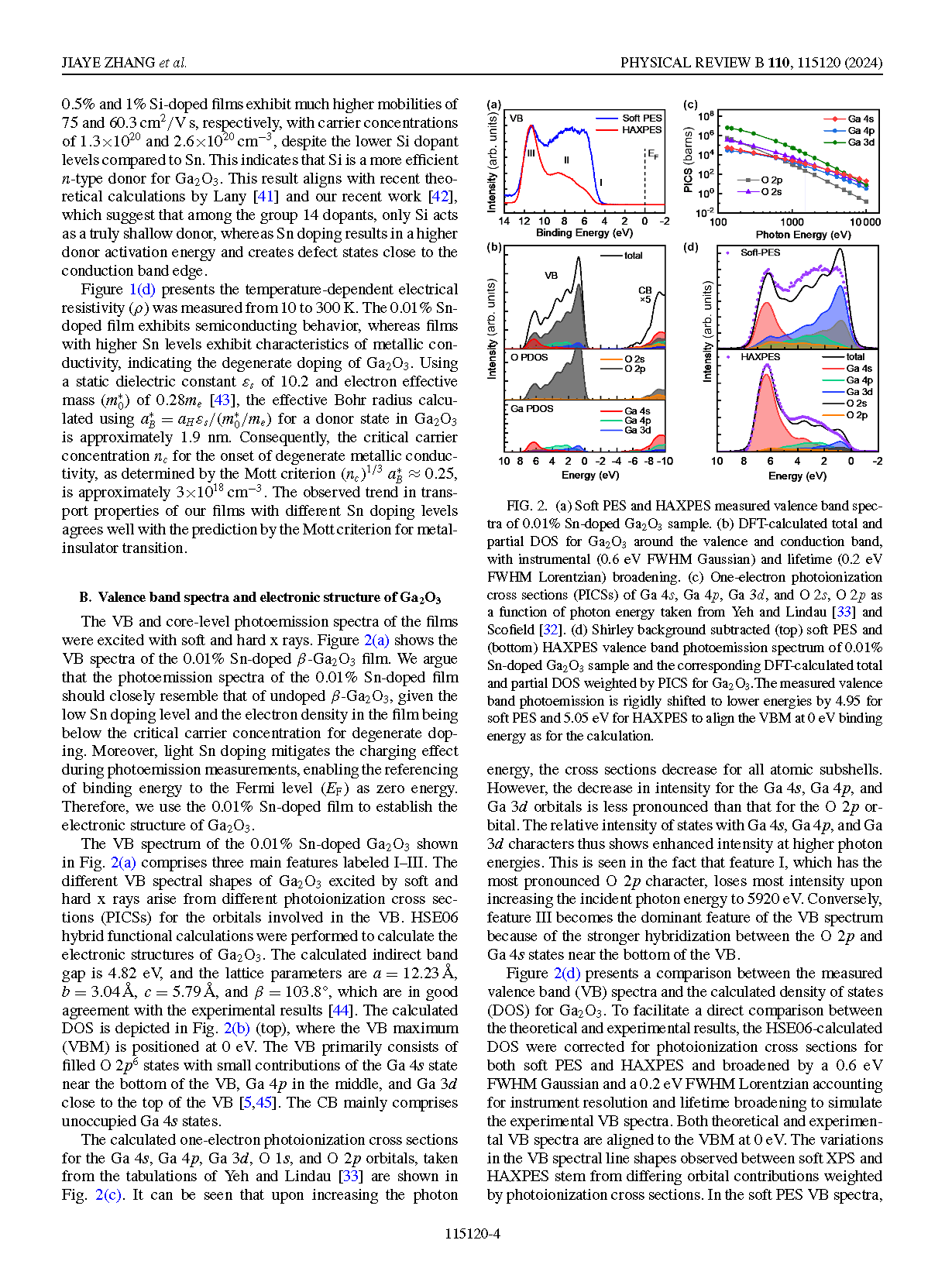
FIG.2. (a) Soft PES and HAXPES measured valence band spectra of 0.01% Sn-doped Ga2O3 sample. (b) DFT-calculated total andpartial DOS for Ga2O3 around the valence and conduction band.with instrumental (0.6 eV FWHM Gaussian) and lifetime (0.2 eV FWHM Lorentzian) broadening.(c) One-electron photoionization cross sections (PICSs) of Ga 4s, Ga 4p, Ga 3d, and O 2s, 0 2p as a function of photon energy taken from Yeh and Lindau and Scofeld. (d) Shirley background subtracted (top) soft PES and (bottom) HAXPES valence band photoemission spectrum of 0.01% Sn-doped Ga2O3 sample and the corresponding DFT-calculated total and partial DOS weighted by PICS for Ga2O3.The measured valence band photoemission is rigidly shifted to lower energies by 4.95 for soft PES and 5.05 eV for HAXPES to align the VBM at 0 eV binding energy as for the calculation.
DOI:
doi.org/10.1103/PhysRevB.110.115120