


Paper Sharing
【Member Papers】 Xidian University --- (001) β-Ga₂O₃ epitaxial layer grown with in-situ pulsed Al atom assisted method by MOCVD
日期:2025-04-03阅读:885
Recently, Associate Professor He Yunlong and Professor Lu Xiaoli from Professor Ma Xiaohua's team at the National Engineering Research Center for Wide Band-gap Semiconductors published a paper entitled "(001) β-Ga2O3 epitaxial layer grown with in-situ pulsed Al atom assisted method by MOCVD " in Journal of Materiomics. This research innovatively proposed pulsed aluminum atom-assisted growth technology, successfully broke through the key technical bottleneck of Gallium Oxide epitaxial material preparation, and laid the foundation for the development of a new generation of high-power electronic devices.、
As a representative of ultra-wide band gap semiconductor materials, Gallium Oxide has important strategic value in the fields of ultra-high voltage power electronics and deep ultraviolet detection. However, when the (001) crystal face β-Ga2O3 epitaxial layer is prepared by metal-organic chemical vapor phase deposition (MOCVD) technology, it is faced with some problems such as high surface roughness and high interface defect density, which seriously restricts the performance and reliability of the device. How to realize the epitaxial growth of thin films with high flatness and low defect has become the focus of research in this field worldwide.
In response to the above challenges, the team researchers innovatively proposed an in situ pulsed aluminum atom-assisted growth method. By precisely regulating the timing and concentration of the pulse injection of aluminum atoms, a triple action mechanism is realized in the epitaxial growth process: directional nucleation, aluminum atoms can be used as the preferred nucleation site to optimize the lattice arrangement orientation; Inhibit side reactions, effectively inhibit the generation and desorption of by-products, reduce oxygen vacancy defect; Interface reconstruction promotes atomic diffusion, weakens random island nucleation, and significantly improves the interface quality between epitaxial layer and substrate.
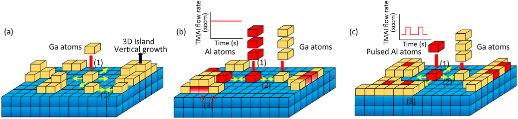
FIG. 1 Schematic diagram of epitaxial growth mechanism
The experimental data show that the surface roughness (RMS) of the epitaxial layer prepared by the new method is reduced by more than 50%, the FWHM of the X-ray rocking curves is reduced to 45.2 arcseconds, and the oxygen vacancy defect density is decreased by an order of magnitude. The research team also observed the phenomenon of epitaxial orientation rotation for the first time, and proposed a theoretical model of the correlation between the rotation Angle and the surface flatness, which provides a new idea for the precise control of the material epitaxial growth.
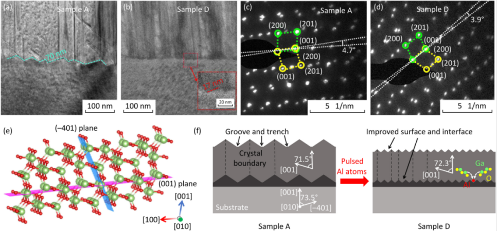
FIG. 2 Test results and principles of HRTEM and SAED
The Schottky Barrier Diode (SBD) prepared based on this technique shows a breakdown field strength of 1.8 MV/cm, which verifies the key role of high-quality epitaxial materials in device performance. The result will strongly support China's independent innovation in the field of ultra-high voltage power electronics, support to break through foreign technical blockades.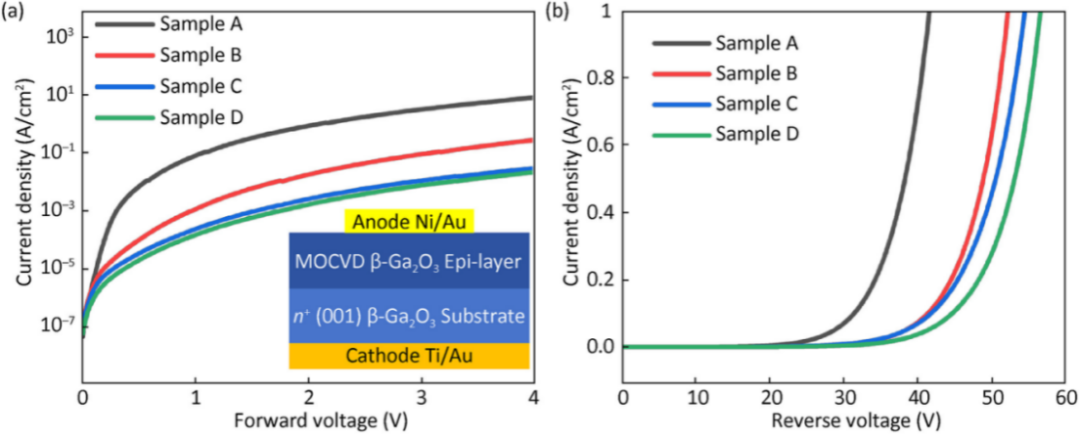
FIG. 3 Forward and reverse IV characteristics of SBD
As an original result of completely independent intellectual property rights, the research team has laid out a number of core patents around pulsed aluminum atom-assisted growth technology, covering key process nodes. At present, the team is working with the industry to promote technology transformation, accelerate the application of Gallium Oxide materials in new energy vehicles, smart grid and other scenarios, and is expected to promote China's wide band gap semiconductor industry to achieve leapfrog development.
Extended Reading
Gallium Oxide (Ga2O3) has a Bandgap of 4.8 eV and a theoretical breakdown field strength 20 times that of silicon, which is regarded as an ideal material for the next generation of high power devices. However, problems such as its high thermal conductivity and low P-type doping difficulty still need further breakthroughs. This study provides important technical support for the engineering application of Gallium Oxide materials.
Paper information:
(001) β-Ga2O3 epitaxial layer grown with in-situ pulsed Al atom assisted method by MOCVD
He, Yunlong; Liu, Yang; Lu, Xiaoli; Wang, Zhan; Song, Xianqiang; Zhou, Ying; Zheng, Xuefeng; Ma, Xiaohua; Hao, Yue
Journal of Materiomics
DOI:10.1016/j.jmat.2024.100981
