Paper Sharing
【International Papers】 Penn State University --- High temperature operation and failure of Ga₂O₃ Schottky barrier diodes: An in situ TEM study
日期:2025-04-03阅读:858
Researchers from the Penn State University have published a dissertation titled "High temperature operation and failure of Ga2O3 Schottky barrier diodes: An in situ TEM study" in APL Electronic Devices.
Corresponding Authors

Aman Haque
He is a Professor of Mechanical Engineering at the Pennsylvania State University. I received my PhD in Mechanical Engineering from the University of Illinois at Urbana Champaign in 2002. Starting as an Assistant Professor in 2003, I was tenured in 2008 and promoted in 2012.
Project Support
The work was performed as part of the Interaction of Ionizing Radiation with Matter University Research Alliance (IIRM-URA), sponsored by the Department of Defense, Defense Threat Reduction Agency under Award No. HDTRA1-20-2-0002.
Background
Gallium oxide (Ga2O3) is a promising ultrawide bandgap material for power electronics and optoelectronics due to its superior physical and electrical properties. However, the poor thermal conductivity of β-Ga2O3 is the bottleneck for its high power and high temperature operation. The β-Ga2O3 is less efficient in dissipating heat compared to other wide bandgap semiconductors such as GaN and SiC due to its anisotropic low thermal conductivity (11–27 Wm−1 K −1). Here, we monitored the real time failure of β-Ga2O3 SBD under forward biasing in the presence of an external thermal field, accomplished by a custom made micro-electro-mechanical system (MEMS) chip.
Abstract
The β-polymorph gallium oxide (Ga2O3) is a promising material for next generation power electronics in extreme environments due to its ultra-wide bandgap with a high theoretical breakdown electric field. However, there is a gap between their predicted and observed reliability at high temperatures or radiation. Here, we investigated the forward bias induced degradation of the β-Ga2O3 Schottky barrier diode (SBD) during high temperature operation. Instead of using conventional post-degradation characterization, we adopted in situ high temperature operation of the β-Ga2O3 SBD inside a transmission electron microscope for real time visualization of the defect nucleation and evolution leading to degradation. The degradation mechanism involves the generation of vacancy clusters and nanoscale amorphized regions by the external and self-heating driven thermal field, which induces higher compressive strain on the β-Ga2O3 crystal. The nanoscale defects created lead to dislocations and stacking fault formation, mostly along the (200) lattice planes, under high temperature biasing conditions. The ultimate breakdown of the diode involves metal pool formation through the intermixing of the Ni/Au Schottky contact metals, which diffuse into the β-Ga2O3 drift layer under high electro-thermal stress. The accumulated defects at the anode metal pool/β-Ga2O3 interface cause highly nonuniform localized strain by void formation, which led to the final breakdown of the diode. The fundamental insights into the defect nucleation and propagation leading to failure may be useful to improve the reliability of β-Ga2O3 based devices for high temperature operation.
Conclusion
We demonstrated the in situ TEM operation of the β-Ga2O3 Schottky barrier diode under high temperature and forward biasing conditions. The real-time visualization of diode failure was achieved using a custom-designed MEMS chip that facilitates simultaneous heating and biasing. Instead of conventional post-failure cross-sectional analysis, this in situ TEM study offers a comprehensive understanding of the nucleation and evolution of defects leading to ultimate failure. The self-heating and external heat induce a large thermal stress on the β-Ga2O3 crystal, generating vacancy clusters as indicated by the higher compressive strain in the lattice. The density of vacancy clusters increases with the increase in biasing temperature, leading to the formation of dislocations, stacking faults, and amorphized regions. Most of the defects, specifically the stacking faults, are generated along the (200) lattice plane due to the lowest thermal conductivity of the β-Ga2O3 in the (100) crystal direction. The high thermoelectric stress degrades the Ni/Au Schottky contact by intermixing and forms a metallic pool of the Au–Ni alloy phase. The anode metallic pool diffuses into the β-Ga2O3 drift layer through the defect paths at the interface. The electro-thermal migration driven Ga rich region and the O vacancy enriched region at the anode, the metal pool, induce a highly non-uniform localized strain field at the metal pool and β-Ga2O3 interface. This leads to the ultimate failure of the device by cracking and delamination. In addition to providing valuable insight into the failure mechanism of β-Ga2O3 SBD under high temperature operation, it also highlights the significance of effective thermal management in enhancing the reliability of β-Ga2O3 based devices. However, we were unable to distinguish the individual effect of self-heating and external heat on the defect nucleation and propagation due to the simultaneous heating and biasing capability of the MEMS chip used here. Further study is required to separate these two effects. In addition, the high temperature reverse bias induced failure mode also needs to be monitored in real time for a more comprehensive understanding of the effect of external thermal load on those devices.
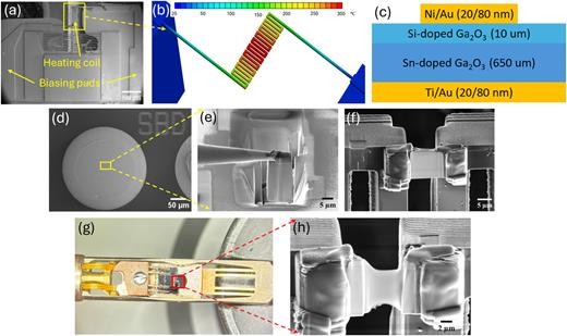
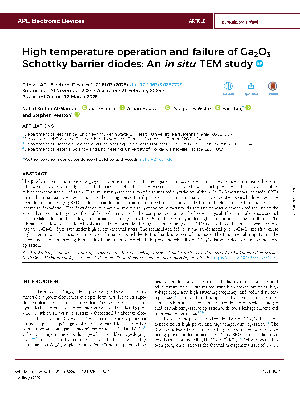
FIG. 1. (a) SEM of the MEMS chip. (b) Ansys result showing the maximum temperature of the MEMS chip at 4 V. (c) Cross-sectional schematic of β-Ga2O3 SBD. (d)–(f) In situ lift out and installation of β-Ga2O3 SBD lamella into the MEMS chip. (g) Protochips heating and biasing holder with the mounted MEMS chip. (h) Electron transparent lamella of β-Ga2O3 SBD.
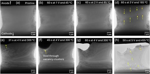
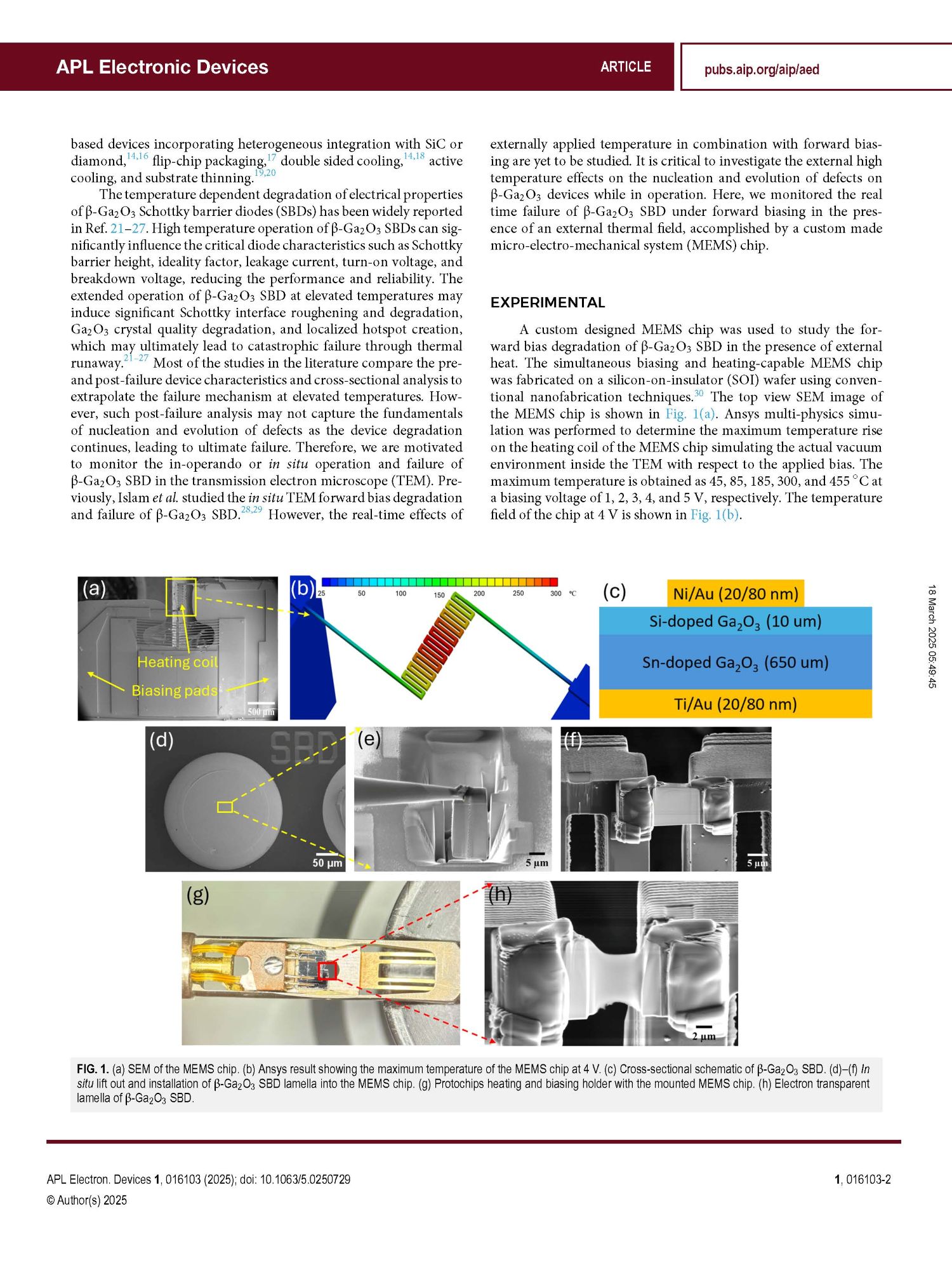
FIG. 2. Low magnification TEM images of the β-Ga2O3 SBD at different biasing conditions: (a) pristine, (b) 60 s at 1 V and 45 °C, (c) 60 s at 2 V and 85 °C, (d) 60 s at 3 V and 185 °C, (e) 31 s at 4 V and 300 °C, (f) 45 s at 4 V and 300 °C, (g) 60 s at 4 V and 300 °C, and (h) 50 s at 5 V and 455 °C.
DOI:
doi.org/10.1063/5.0250729