Paper Sharing
【International Papers】Thermally induced PtOx interfacial layer enhances stability of Pt/β-Ga₂O₃ vertical Schottky diodes
日期:2025-04-09阅读:806
Researchers from the National Renewable Energy Laboratory have published a dissertation titled "Thermally induced PtOx interfacial layer enhances stability of Pt/β-Ga2O3 vertical Schottky diodes" in APL Energy.
Acknowledgments
This work was authored by the National Renewable Energy Laboratory (NREL), operated by Alliance for Sustainable Energy, LLC, for the U.S. Department of Energy (DOE) under Contract No. DE-AC36-08GO28308. Funding was provided by the Office of Energy Efficiency and Renewable Energy (EERE), Advanced Materials and Manufacturing Technologies Office for high-temperature experiments, and NREL’s Laboratory Directed Research and Development (LDRD) program for high voltage experiments. C. Chae and J. Hwang acknowledge funding support from microscopy analysis by the Intel® Semiconductor Education and Research Program for Ohio.
Abstract
This study investigates the long-term stability of Pt/β-Ga2O3 field-plated Schottky barrier diodes at high temperatures, with extended thermal cycling and soaking stress. The device characteristics reveal a strong dependence on operating temperature, leading to an ON/OFF current ratio of ∼10× at ±3 V and 600 °C. Extensive thermal cycling (25 cycles over 100 h) between room temperature and 350 °C shows that leakage currents stabilize after the initial ten cycles. This stabilization is likely due to the formation of a thin PtOx layer at the Pt/β-Ga2O3 interface, as confirmed by high-resolution scanning transmission electron microscopy. Further exposure to a constant 350 °C environment for 10 h reveals a slight increase in the leakage current from 10−7 to 10−6 A at −5 V and degradation of the forward current, due to potential thermodynamic instability of the Ohmic contacts. This study provides insights into the changes in the Pt/β-Ga2O3 diode performance with thermal stress, offering a basis for predicting the device’s operational reliability at high temperatures for sensing and power applications.
Conclusion
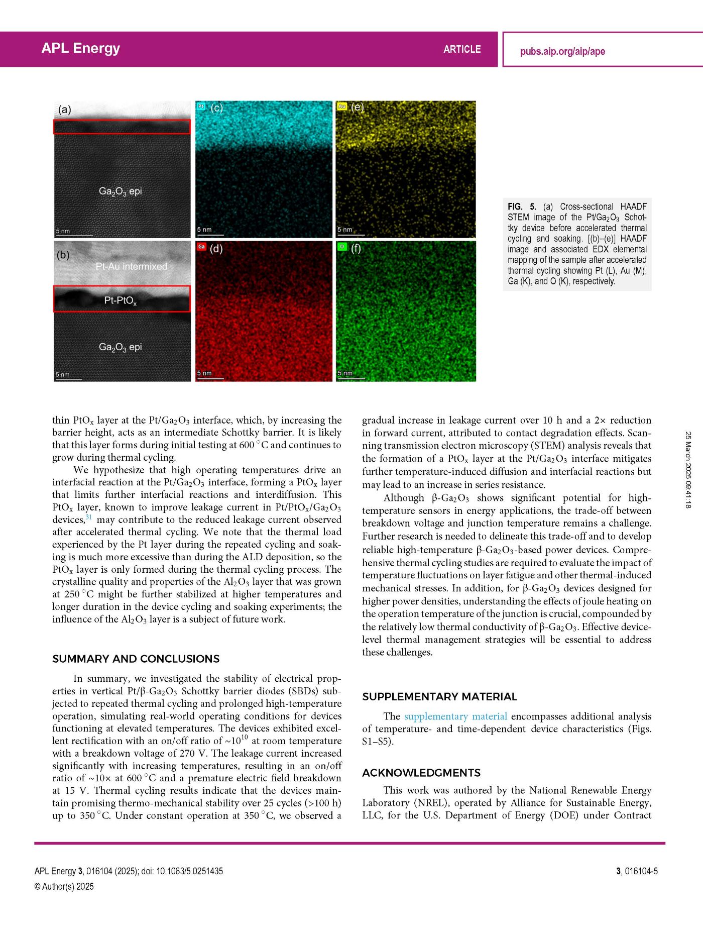
In summary, we investigated the stability of electrical properties in vertical Pt/β-Ga2O3 Schottky barrier diodes (SBDs) subjected to repeated thermal cycling and prolonged high-temperature operation, simulating real-world operating conditions for devices functioning at elevated temperatures. The devices exhibited excellent rectification with an on/off ratio of ∼1010 at room temperature with a breakdown voltage of 270 V. The leakage current increased significantly with increasing temperatures, resulting in an on/off ratio of ∼10× at 600 °C and a premature electric field breakdown at 15 V. Thermal cycling results indicate that the devices maintain promising thermo-mechanical stability over 25 cycles (>100 h) up to 350 °C. Under constant operation at 350 °C, we observed a gradual increase in leakage current over 10 h and a 2× reduction in forward current, attributed to contact degradation effects. Scanning transmission electron microscopy (STEM) analysis reveals that the formation of a PtOx layer at the Pt/Ga2O3 interface mitigates further temperature-induced diffusion and interfacial reactions but may lead to an increase in series resistance.
Although β-Ga2O3 shows significant potential for high-temperature sensors in energy applications, the trade-off between breakdown voltage and junction temperature remains a challenge. Further research is needed to delineate this trade-off and to develop reliable high-temperature β-Ga2O3-based power devices. Comprehensive thermal cycling studies are required to evaluate the impact of temperature fluctuations on layer fatigue and other thermal-induced mechanical stresses. In addition, for β-Ga2O3 devices designed for higher power densities, understanding the effects of joule heating on the operation temperature of the junction is crucial, compounded by the relatively low thermal conductivity of β-Ga2O3. Effective device-level thermal management strategies will be essential to address these challenges.
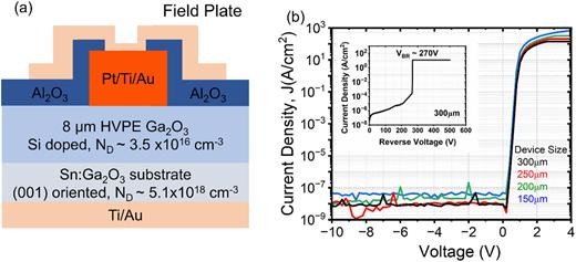
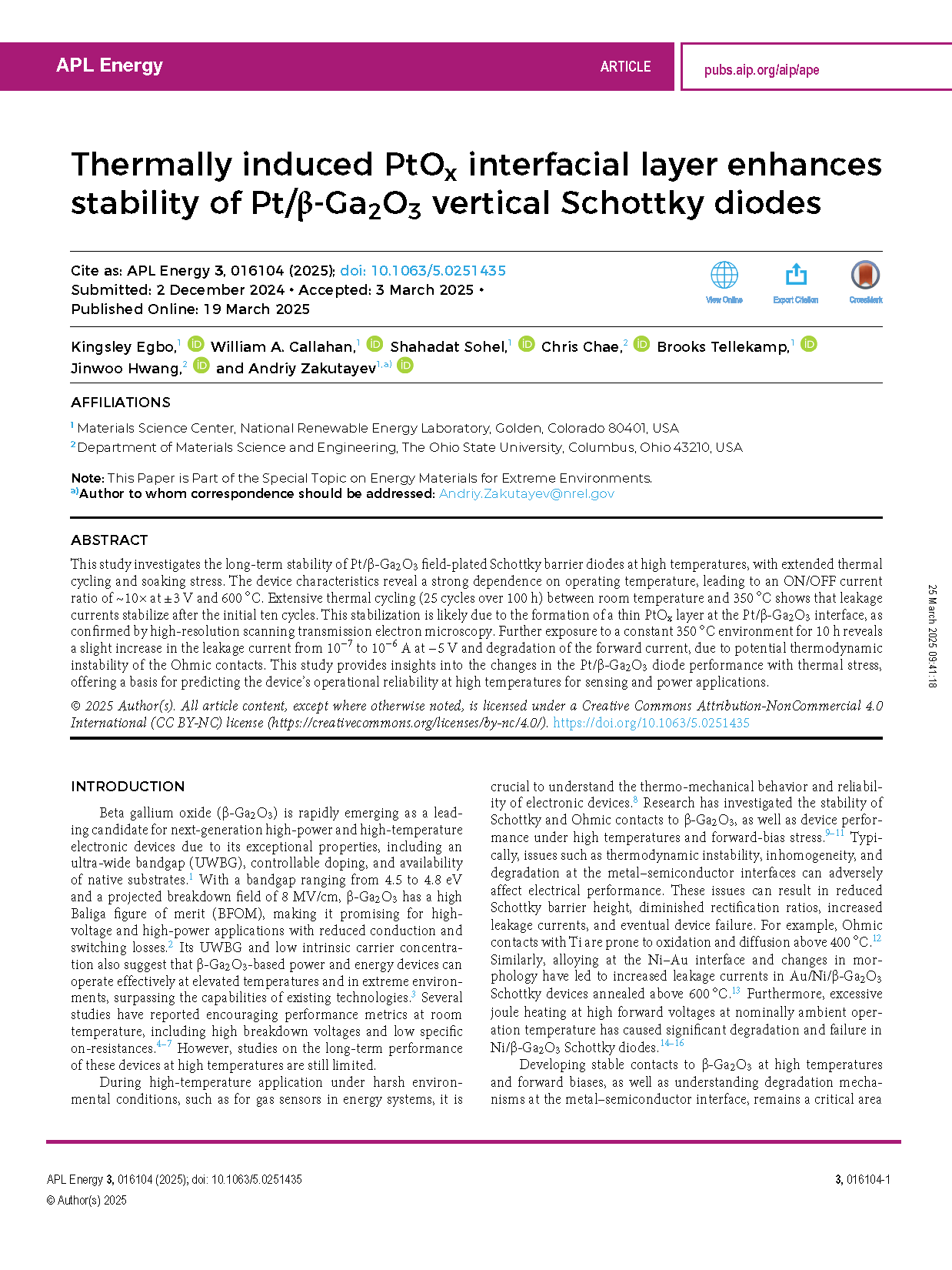
FIG. 1. (a) Schematic of the fabricated vertical HVPE (001) β-Ga2O3 field-plate Schottky diode structure. (b) Room temperature current–voltage (J–V) measurements of different pad sizes. The inset shows the room temperature 300 μm device breakdown of ∼270 V.
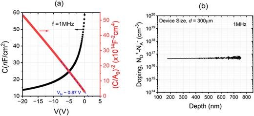
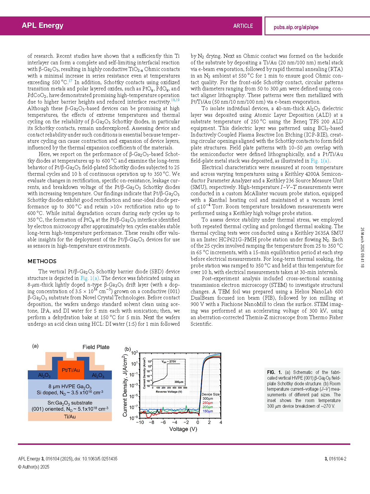
FIG. 2. (a) Capacitance–voltage (C–V) characteristics of the vertical Schottky barrier diode showing a built-in voltage of ∼0.87 eV. (b) Measured net doping concentration of the (001) β-Ga2O3 drift layer extracted from the C–V measurement.
DOI:
doi.org/10.1063/5.0251435