


Paper Sharing
【Domestic Papers】Jilin University --- Silicon-Based Gallium Oxide Optical Waveguide Fabricated by MOCVD
日期:2025-04-09阅读:810
Researchers from the Jilin University have published a dissertation titled "Silicon-Based Gallium Oxide Optical Waveguide Fabricated by MOCVD" in Vacuum.
Acknowledgments
This work was supported by the Natural Science Foundation of Jilin Province under Grant 20230101124JC.
Background
Photonic integrated circuit (PIC) is a type of integrated circuit technology based on the principles of photonics for information transmission and processing. In comparison with traditional electronic integrated circuits, photons (i.e., quanta of light) are used as the medium for transmitting and processing information in the photonic integrated circuit. PIC exhibits higher bandwidth, lower power consumption, and higher speeds, making it highly promising for high-speed communications. In recent years, PIC based on silicon photonics has attracted significant attention due to silicon's excellent optical properties and its compatibility with well-developed CMOS processes. However, the narrower bandgap (1.18 eV) of silicon limits the effective transmission wavelength range to the infrared region. It restricts the potential applications of silicon in shorter wavelengths, such as in the visible and UV regions. Gallium oxide (Ga2O3) is an ultra-wideband semiconductor material with a bandgap of 4.6 eV–5.1 eV, a dielectric constant ranging from 10.2 to 14.2, and excellent thermal and chemical stability. Ga2O3 has been widely studied in the fields of power electronics and solar-blind UV detection. Ga2O3 could provide broadband transparency in the UV-NIR spectral range. The excellent optical properties make it highly promising for integrated photonic devices operating within the UV-NIR spectral, including frequency metrology, on-chip mode-locking and visible communication.
Abstract
In this paper, the Ga2O3 films were grown on Si/SiO2 template by MOCVD and the effects of the growth temperature on the film's properties were investigated. The films transitioned from an amorphous phase to a polycrystalline β-Ga2O3 phase as the growth temperature increased. The bonding state of oxygen in the films was investigated. Based on the measured optical parameters of amorphous Ga2O3 films and optical simulation calculation, optical waveguide structures were designed and fabricated. The characteristics of the waveguide were consistent with the design. The 2.5-μm-wide, 310-nm-high Ga2O3 waveguide achieved an optical loss of 12.4 dB/cm at 1550 nm using the truncation method. This study demonstrated that amorphous Ga2O3 films grown by the MOCVD have great potential for waveguide fabrication.
Highlights
·On-chip waveguide utilizing amorphous Ga2O3films was successfully fabricated and presented good waveguide performance.
·Ga2O3thin films with smooth surfaces have been successfully epitaxially grown on Si/SiO2template by MOCVD.
·The bonding state of oxygen in Ga2O3films grown on Si/SiO2 template under different temperatures have been researched.
Conclusions
The amorphous and polycrystalline Ga2O3 films were grown on Si/SiO2 template using MOCVD. The surface morphology and roughness, crystalline quality, atomic composition, bonding configuration, and refractive index of the Ga2O3 films were characterized. As the growth temperature increased, the films transitioned from amorphous to polycrystalline β-Ga2O3 phase. By optimizing the growth temperature, smooth amorphous Ga2O3 films with RMS roughness of 0.77 nm were obtained. XPS analysis showed higher off-lattice oxygen content in amorphous films, correlating with their disordered atomic configurations. The refractive index of the amorphous Ga2O3 films grown at 510 °C was measured to be 1.878 at a wavelength of 1550 nm. The optical transmission loss of the fabricated Ga2O3 waveguide at 1550 nm was measured to be 12.4 dB/cm using the truncation method. Near-field output images indicated that the Ga2O3 optical waveguides operated in the fundamental mode. The Ga2O3 films as an excellent material have great application potential in the production of on-chip waveguides.
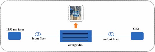
Fig. 1. Schematic diagram of waveguide transmission loss test system.
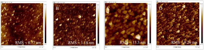
Fig. 2. AFM images of Ga2O3 films grown at different temperatures (A: 510 °C; B: 600 °C; C: 675 °C; D: 750 °C).
DOI:
doi.org/10.1016/j.vacuum.2025.114221
