Paper Sharing
【Member Papers】Xidian University --- Forward bias stress-induced degradation mechanism in β-Ga₂O₃ SBDs: A trap-centric perspective
日期:2025-04-09阅读:940
Researchers from the Xidian University have published a dissertation titled "Forward bias stress-induced degradation mechanism in β-Ga2O3 SBDs: A trap-centric perspective" in Applied Physics Letters.
Project Support
This work was supported by the National Key Research and Development Program of China (Grant No. 2023YFB3611902), the National Natural Science Foundation of China (Grant Nos. 62104180, U2241220, and 62421005), the Natural Science Basic Research Plan in Shaanxi Province of China (Grant No. 2023-JCQN-0669), and by the fund of National Innovation Center of Radiation Application (Grant No. KFZC2022020401).
Background
β-Gallium oxide (β-Ga2O3) has emerged as a promising material for high-power electronic devices, including Schottky barrier diodes (SBDs), owing to its exceptional properties such as an ultrawide bandgap (4.5–4.9 eV) and high critical electric field strength (8MV/cm). However, these devices suffer from degradation under forward bias stress, which affects their long-term reliability. This study investigates the degradation mechanism of β-Ga2O3 SBDs under FBS, with a specific focus on trap-related physical processes.
Abstract
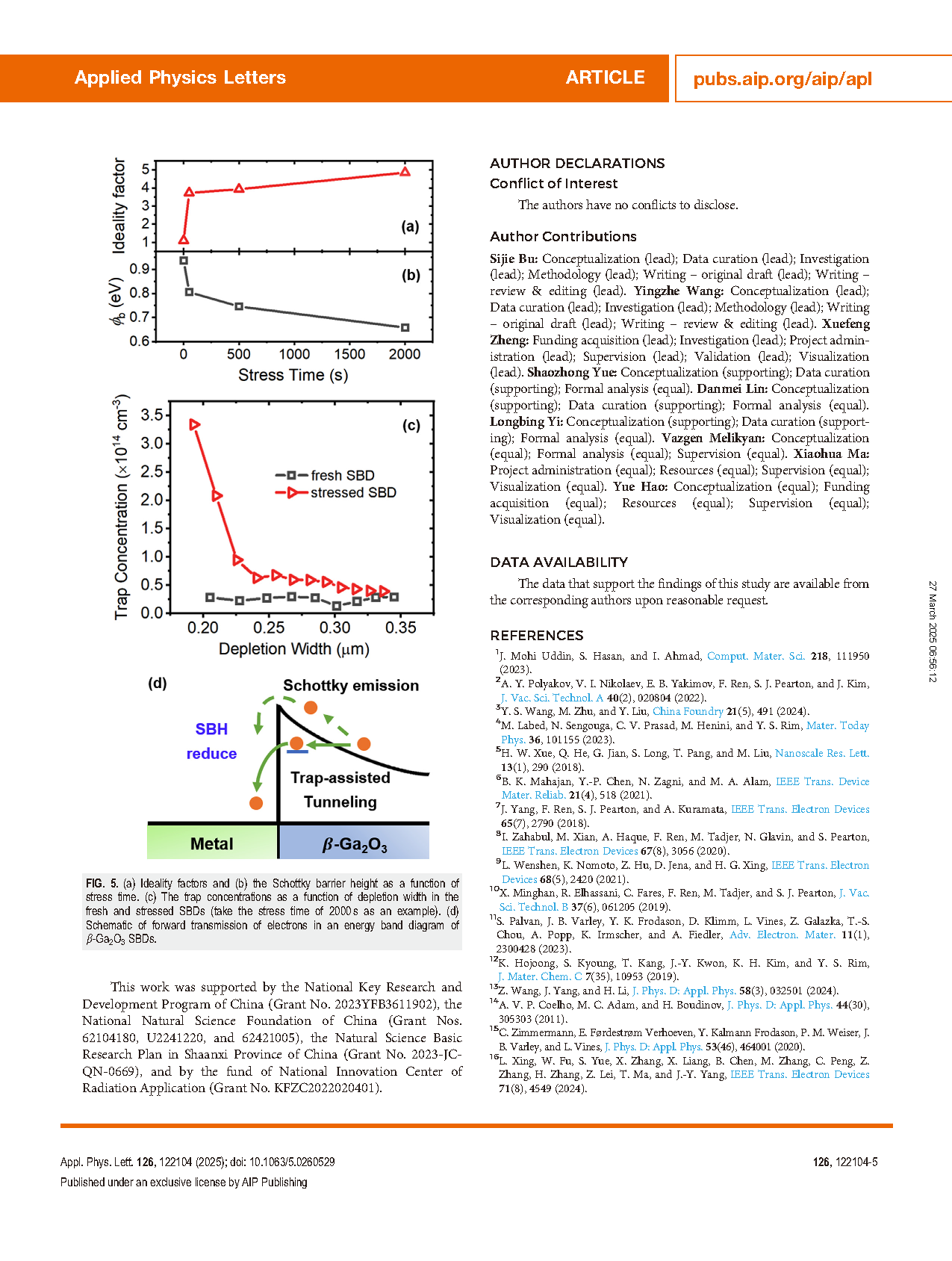
This study explores the impact of constant forward electrical stress on beta-gallium oxide (β-Ga2O3) Schottky barrier diodes (SBDs) from the prospective of defect evolution. Prolonged stress significantly increased the reverse leakage current density (JR) and forward current density (JF) under small bias and decreased the turn-on voltage (Von). Temperature-dependent current-voltage (I-V-T) analysis revealed that the reverse leakage current is dominated by Poole-Frenkel (PF) emission in both fresh and stressed SBDs, while the forward current transport mechanism transforms from thermionic emission (TE) to trap-assisted tunneling (TAT) after stress. Deep-level transient spectroscopy (DLTS) results identified an intrinsic trap E2* (EC - 0.75 eV) within the β-Ga2O3 drift layer, which is likely a Ga vacancy-related trap. The consistency of this energy level with the PF barrier proves that the increase in this trap is the main reason for the increase in JR. The spatial distribution features that the increase in trap concentration near the metal-semiconductor interface is much larger than that inside the bulk, which establishes the association between this trap and JF under small bias and Von. These findings highlight the critical role of trap evolution in SBD performance degradation under electrical stress.
Conclusion
In summary, this work investigated the degradation mechanism of β-Ga2O3 SBDs under forward electrical stress. With increasing stress time, both the reverse current and the forward current at small bias increased, and the turn-on voltage decreased. By delving into the conduction mechanism and trap characterization using DLTS measurement, we identified that the increase in traps E2*, associated with VGa at EC-0.75 eV, leads to an increase in the reverse current dominated by the PF emission mechanism. A more significant increase in trap concentration near the metal-semiconductor interface results in an effective reduction of the equivalent Schottky barrier height, thus increasing the forward current at small bias and causing a negative drift in the turn-on voltage. Interestingly, a quasi-exponential trap distribution extending from the interface was observed and correlated with the degradation of the electrical properties in β-Ga2O3 SBDs. This study establishes a relationship between trap concentration, the spatial distribution of traps, and device performance over stress time, providing valuable insights for enhancing the reliability of β-Ga2O3 SBDs.
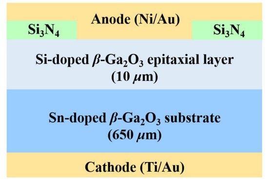
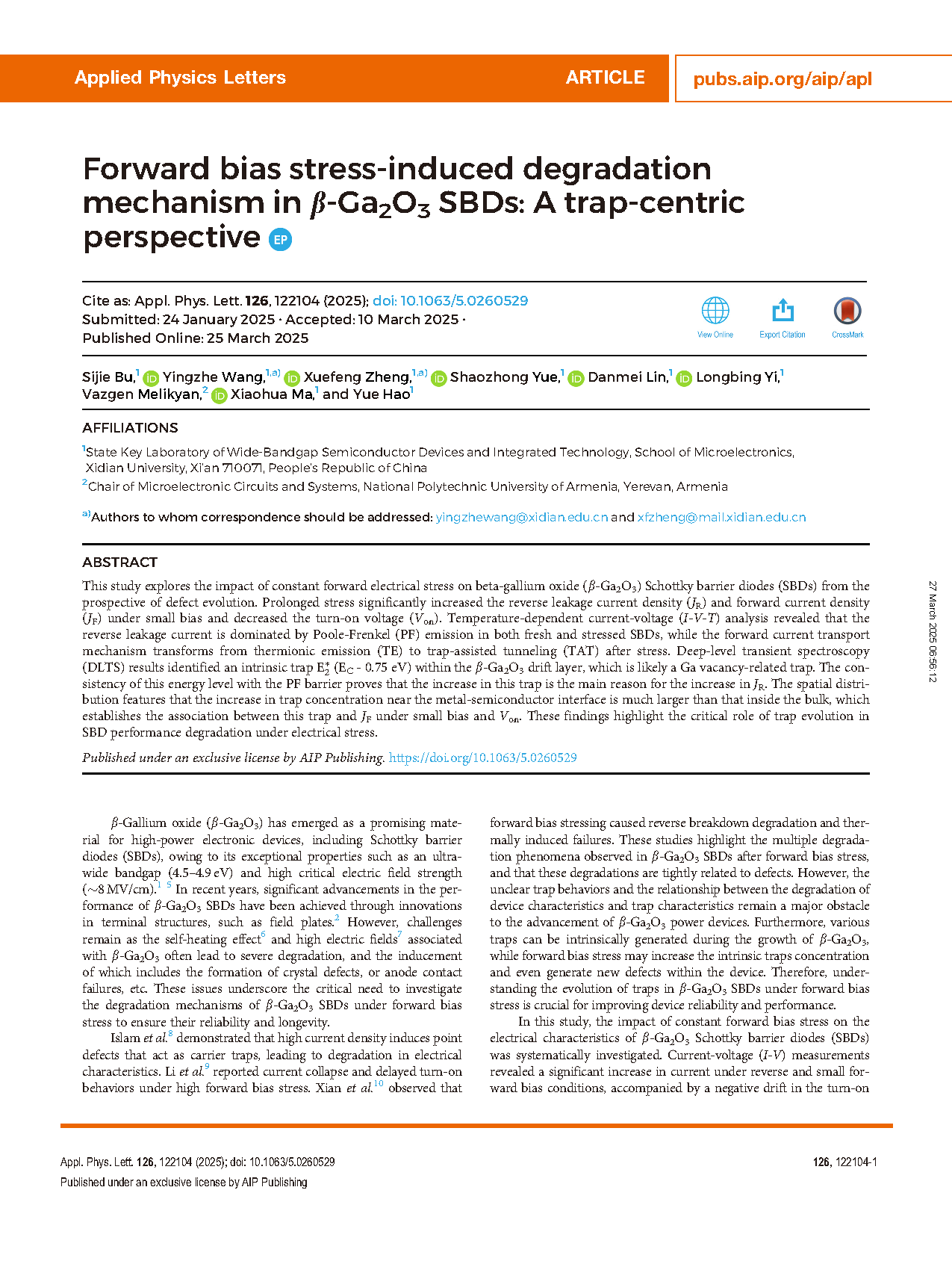
FIG. 1. Schematic cross section of field plate structure β-Ga2O3 SBDs.
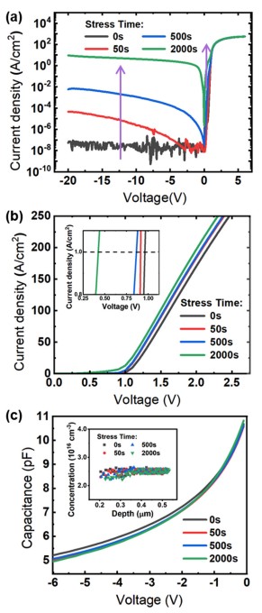
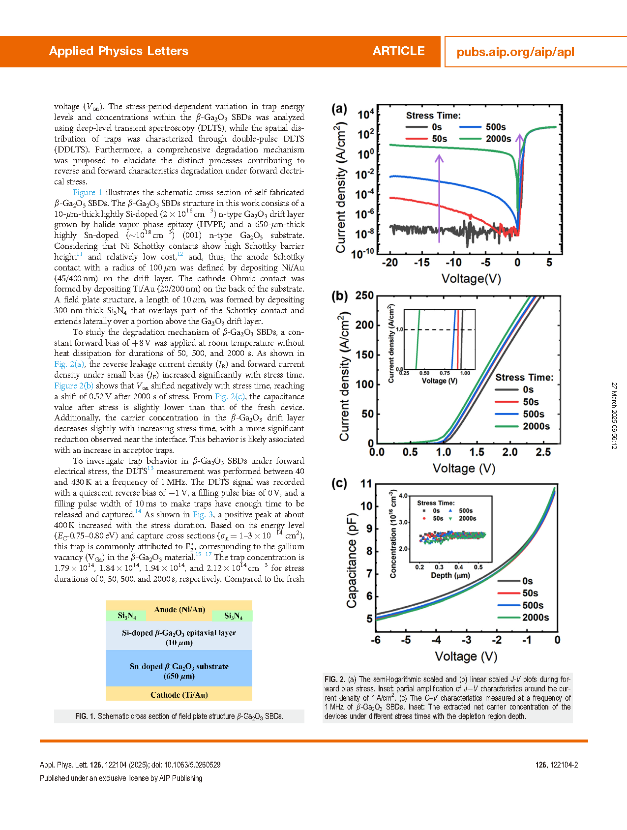
FIG. 2. (a) The semi-logarithmic scaled and (b) linear scaled J-V plots during forward bias stress. Inset: partial amplification of J-V characteristics around the current density of 1 A/cm2. (c) The C–V characteristics measured at a frequency of 1 MHz of β-Ga2O3 SBDs. Inset: The extracted net carrier concentration of the devices under different stress times with the depletion region depth.
DOI:
doi.org/10.1063/5.0260529