Paper Sharing
【Domestic Papers】High-temperature N ion implantation for performance-enhanced current-blocking layers in β-Ga₂O₃
日期:2025-04-13阅读:858
Researchers from the Sun Yat-sen University have published a dissertation titled " High-temperature N ion implantation for performance-enhanced current-blocking layers in β-Ga2O3" in Applied Physics Letters.
Project Support
This work was supported in part by the National Key Research and Development Program of China (Grant No. 2024YFE0205300) and the National Natural Science Foundation of China (Grant No. 62471504). The authors gratefully acknowledge technical support from the Laboratory Teaching Center of Electronics and Information Technology at Sun Yat-sen University and the Nano Fabrication Facility and Vacuum Interconnected Nanotech Workstation (NANO-X) of the Suzhou Institute of Nano-Tech and Nano-Bionics, Chinese Academy of Sciences.
Background
Beta gallium oxide (β-Ga2O3) is regarded as a strong candidate for next-generation power electronics due to its exceptional material properties, including an ultra-wide bandgap of 4.8 eV, a high breakdown electric field of 8MV/cm, and a Baliga figure of merit (BFOM) of 3444. Furthermore, β-Ga2O3 offers excellent chemical stability and radiation resistance, making it ideal for electronic devices in harsh environments. Another major advantage of β-Ga2O3 is its capability to produce large single crystals via melt growth methods, such as the floating zone (FZ) technique and edge-defined film-fed growth (EFG) technique, which enables manufacturing cost reduction.
It has been reported that ion implantation doping at elevated temperatures offers an in situ dynamic annealing effect, bringing several benefits, including reducing the implantation-induced damage and achieving a high impurity activation efficiency, especially to the wide bandgap semiconductors such as SiC and GaN. However, such studies are rare in the field of β-Ga2O3. In this work, we investigate the effects of implantation temperatures and postimplantation annealing (PIA) on the structural and electrical properties of N-implanted β-Ga2O3, demonstrating performance-enhanced CBLs and MOSFETs through N high-temperature implantation (HTI) over the room-temperature implantation (RTI) with PIA.
Abstract
This work reveals the significant advantages of high-temperature nitrogen (N) ion implantation for fabricating current-blocking layers (CBLs) in β-Ga2O3. A comparative investigation on the structural and electrical properties of N-implanted β-Ga2O3 was conducted under different implantation temperatures and post-implantation annealing (PIA) conditions. The results showed that the high-temperature implantation (HTI) at 500 °C, compared to the room-temperature implantation (RTI), introduced fewer structural defects and less lattice distortion to β-Ga2O3. The HTI-formed CBL demonstrated a far superior current-blocking capability than those formed by the RTI with/without a PIA, in terms of a much lower and more stable leakage current and a significantly enhanced breakdown voltage. Additionally, lateral MOSFETs fabricated with the HTI isolation exhibited a three orders of magnitude lower off-state leakage current while maintaining excellent on-state performance, compared to those using the isolation formed by RTI with PIA. These findings indicate that the in situ dynamic annealing effect of HTI effectively reduces implantation-induced damage, enhances impurity activation, and improves the overall performance of the N-implanted CBLs in β-Ga2O3.
Summary
In conclusion, we have demonstrated performance-enhanced CBLs through implanting N ions into β-Ga2O3 at a high temperature of 500 °C. Compared to RTI with PIA, the HTI process effectively reduces the implantation-induced damage, maintains a good surface morphology, and enhances the impurity activation efficiency. The CBLs fabricated by HTI exhibited much lower and more stable leakage currents, as well as significantly improved breakdown voltages. Moreover, the lateral MOSFETs based on an HTI CBL showed a three orders of magnitude lower off-state leakage current and good on-state performance. These findings highlight the significant advantages of the HTI process in fabricating β-Ga2O3 power devices.
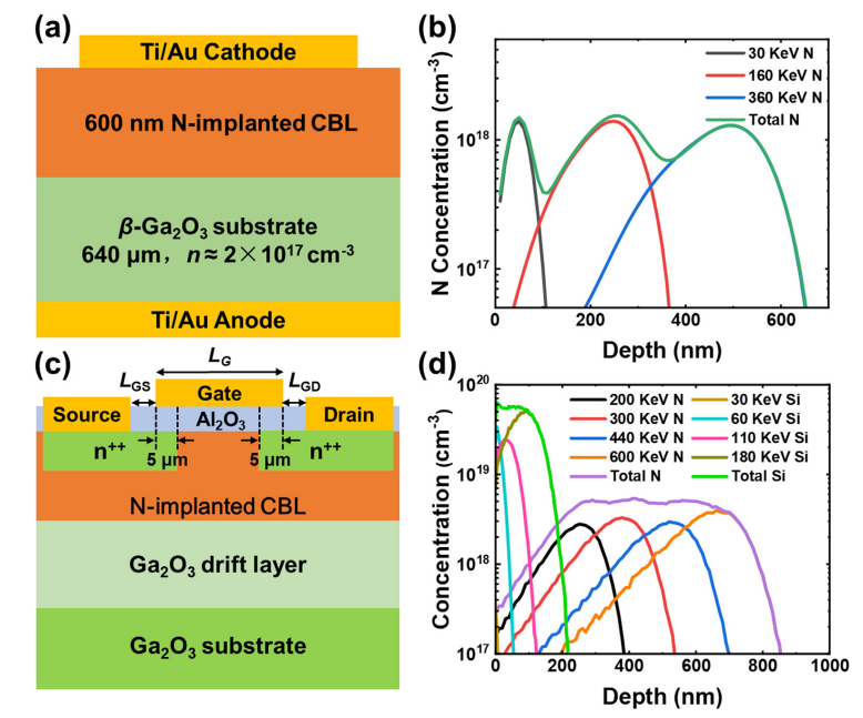
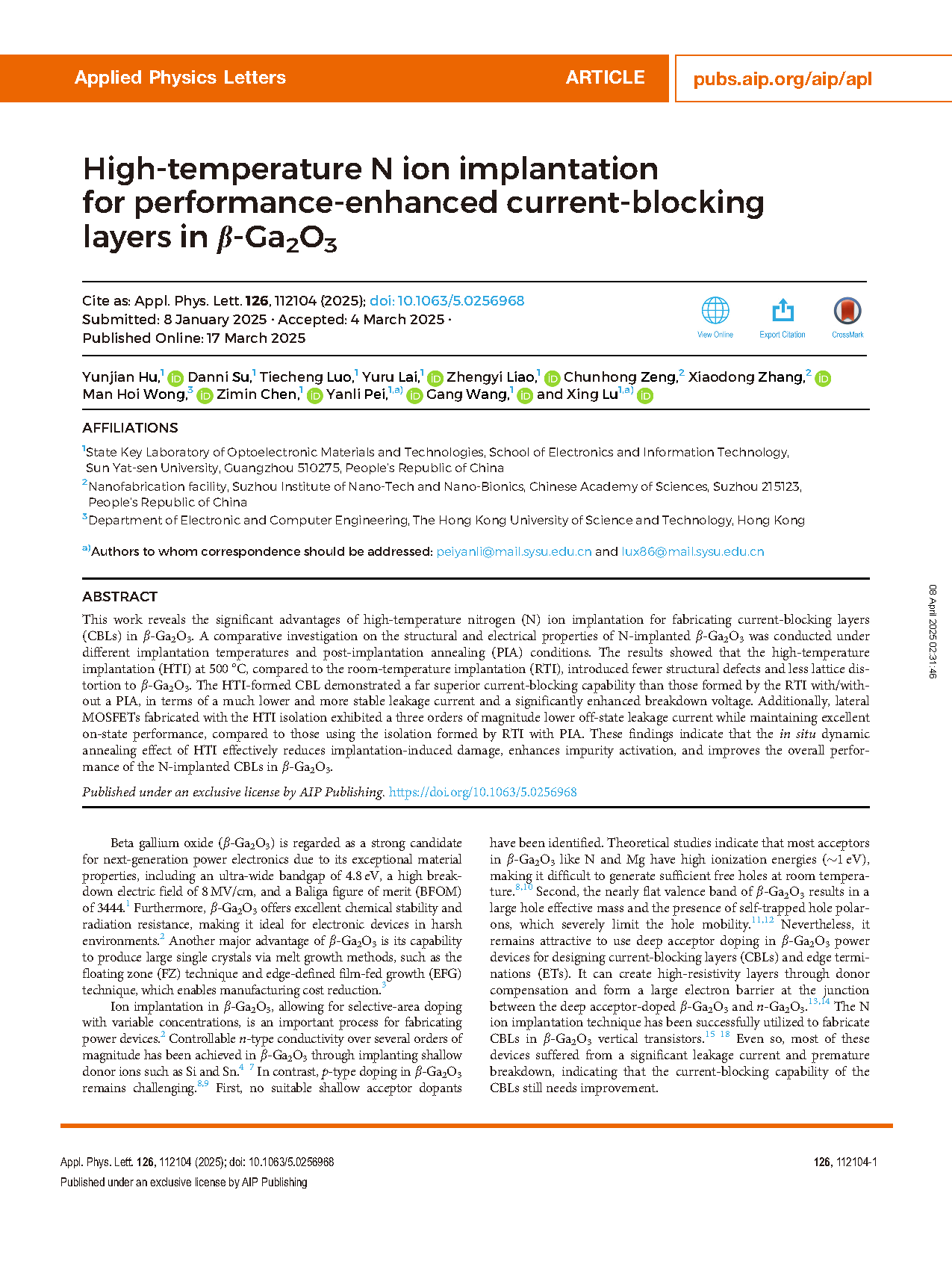
FIG. 1. (a) Cross-sectional schematic of the CBL/n-Ga2O3 structure and (b) the corresponding SRIM-simulated depth distribution of N ion implantation. (c) cross-sectional schematic of the lateral MOSFET fabricated with a N-implanted isolation and (d) the corresponding SRIM-simulated depth distribution of N and Si ion implantation.
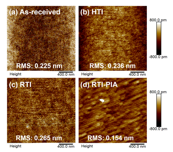
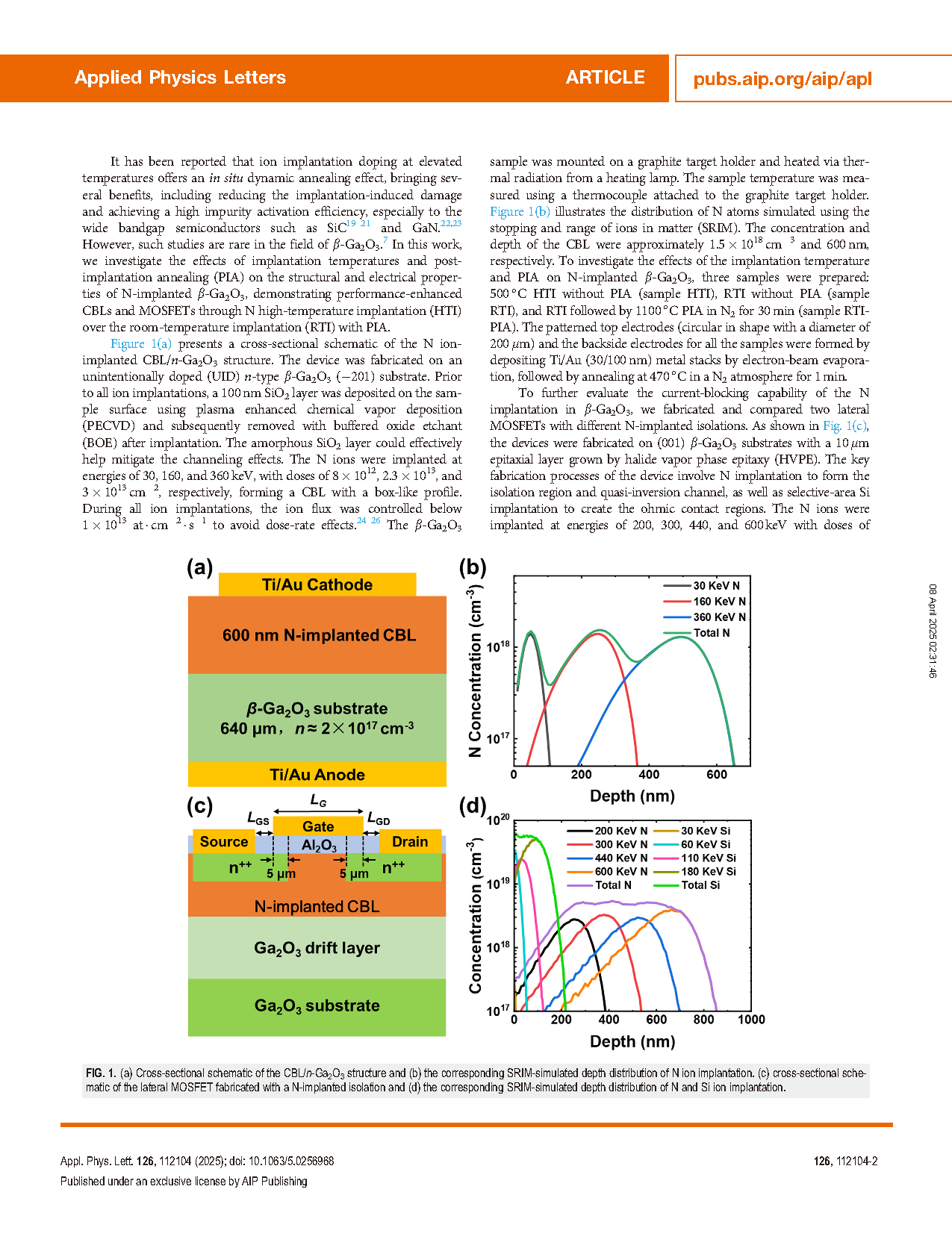
FIG. 2. AFM images of (a) as-received sample, (b) HTI sample, (c) RTI sample, and (d) RTI-PIA sample.
DOI:
doi.org/10.1063/5.0256968