


Paper Sharing
【Device Papers】Formation of Ga₂O₃ and NiO Thin Films at Low Process Temperatures for PN Heterojunction Diodes
日期:2025-04-27阅读:786
Researchers from the Korea Aerospace University have published a dissertation titled "Formation of Ga2O3 and NiO Thin Films at Low Process Temperatures for PN Heterojunction Diodes" in ACS Applied Electronic Materials.
Abstract
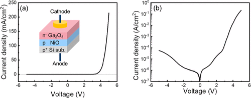
A heterojunction consisting of n-type Ga2O3 and p-type NiO thin films is fabricated at low process temperatures. This technology offers the potential to improve heterojunction applications with wide bandgap semiconductors on various substrates. Optical bandgap values of 4.67 and 3.62 eV are obtained for the Ga2O3 and NiO semiconductors, respectively, from a Tauc plot. The spontaneously formed depletion region in the heterojunction has capacitive characteristics under thermal equilibrium conditions, while the resistive component is involved in the charge transport under the turn-on voltage ranges. The maximum electric field at the heterojunction interface with 50 nm thick n-Ga2O3 is five times higher than that of the n-Ga2O3 with a thickness of over 400 nm under thermal equilibrium conditions. When the junction thickness becomes shorter than the junction depletion width, the diode suffers from an early breakdown due to the much higher maximum electric field at the PN junction interface.
DOI:
https://doi.org/10.1021/acsaelm.5c00092
