Paper Sharing
【Member Papers】Xiamen University---Increase fixed charge at Al₂O₃/Ga₂O₃ interface for high-performance Ga₂O₃ trench Schottky barrier diodes by atomic nitrogen treatment
日期:2025-04-27阅读:876
Researchers from the Xiamen University have published a dissertation titled "Increase fixed charge at Al2O3/Ga2O3 interface for high-performance Ga2O3 trench Schottky barrier diodes by atomic nitrogen treatment" in Applied Physics Letters.
Project Support
This work was supported by the National Natural Science Foundation of China (Grant No. 62171396) and the Shenzhen Science and Technology Program (Grant No. JCYJ20240813145617023).
Background
β-Ga2O3, with its wide bandgap (4.5–4.9 eV) and high theoretical breakdown field (8 MV/cm), has emerged as a promising material for high-voltage and high-power applications. Compared to conventional wide bandgap semiconductors such as GaN and SiC, β-Ga2O3 offers significant advantages, including lower production costs due to its cost-effective melt growth method. This cost advantage makes β-Ga2O3 particularly attractive for large-scale commercial applications. Generally, conventional planar Ga2O3 Schottky barrier diodes (SBDs) suffer from severe electric field crowding at the Schottky contact edges under reverse bias, which triggers premature breakdown and elevates reverse leakage currents. However, trench Schottky barrier diode (TSBD) architecture tackles this challenge innovatively. By vertically embedding the Schottky contact within the trench structure, TSBDs effectively redistribute the electric field away from the contact periphery, thereby suppressing field crowding and enhancing the effective breakdown strength. Such fundamental improvements over planar architectures solidify TSBDs as a critical enabler for β-Ga2O3 to transcend the limitations of conventional SBDs in high-voltage scenarios.
Abstract
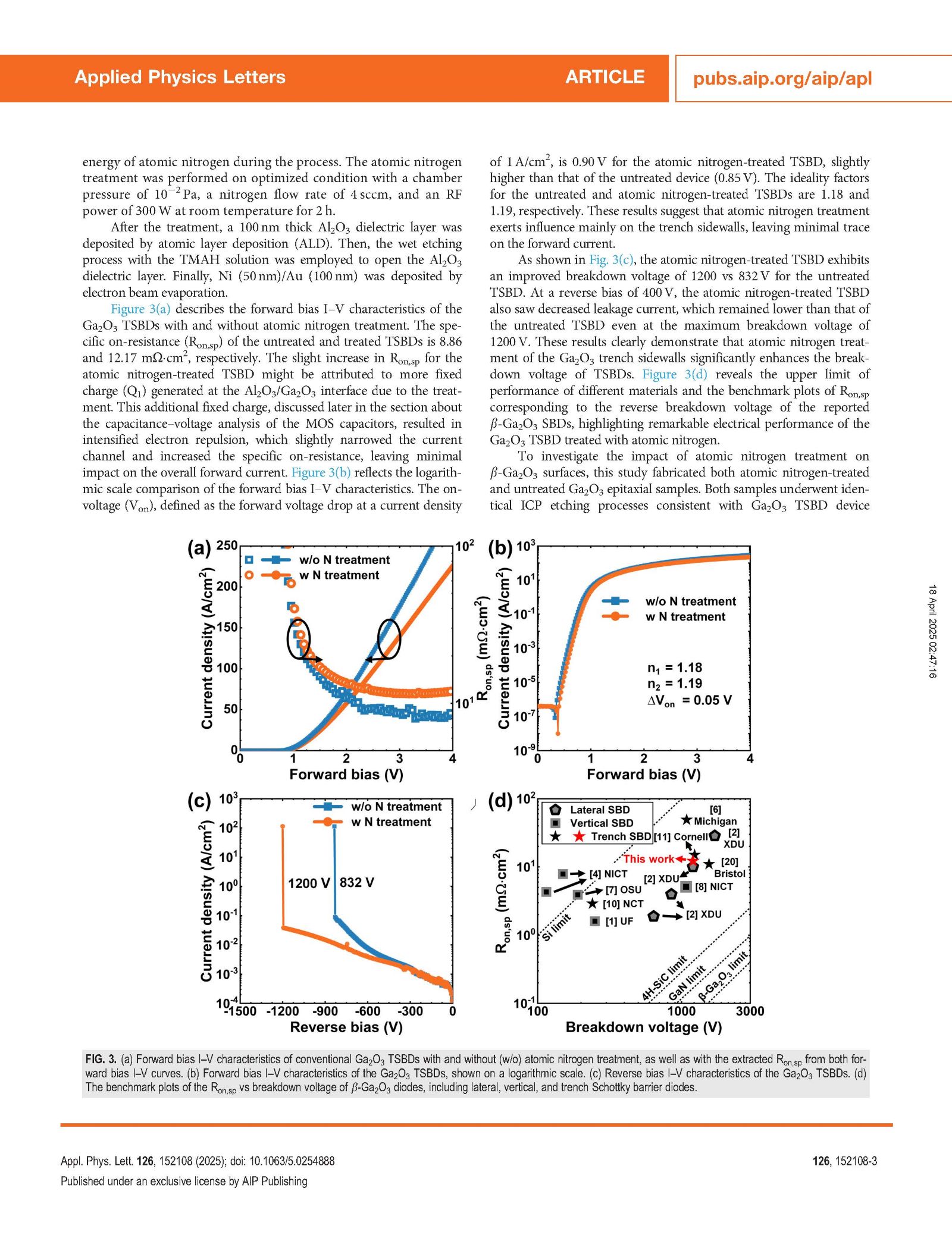
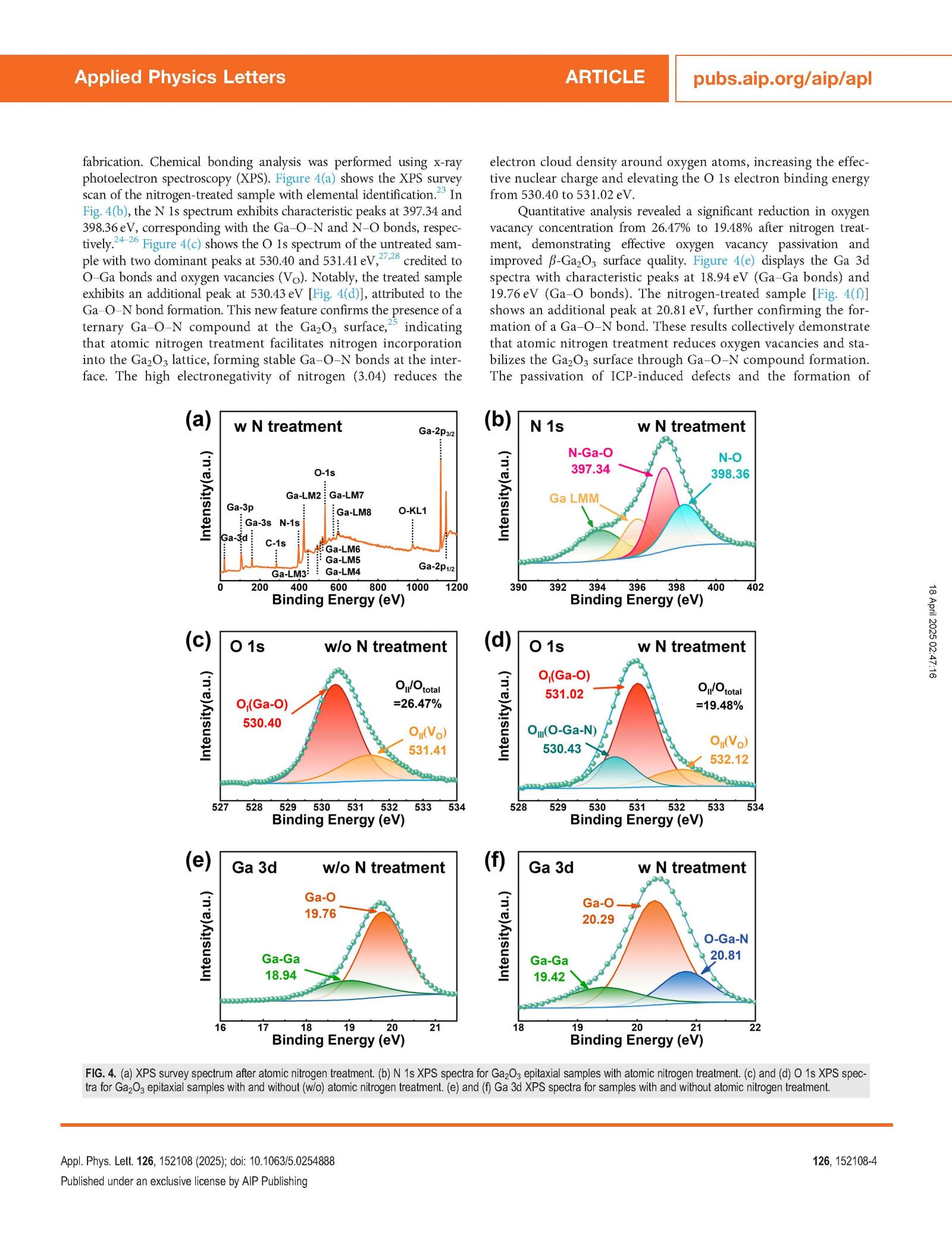
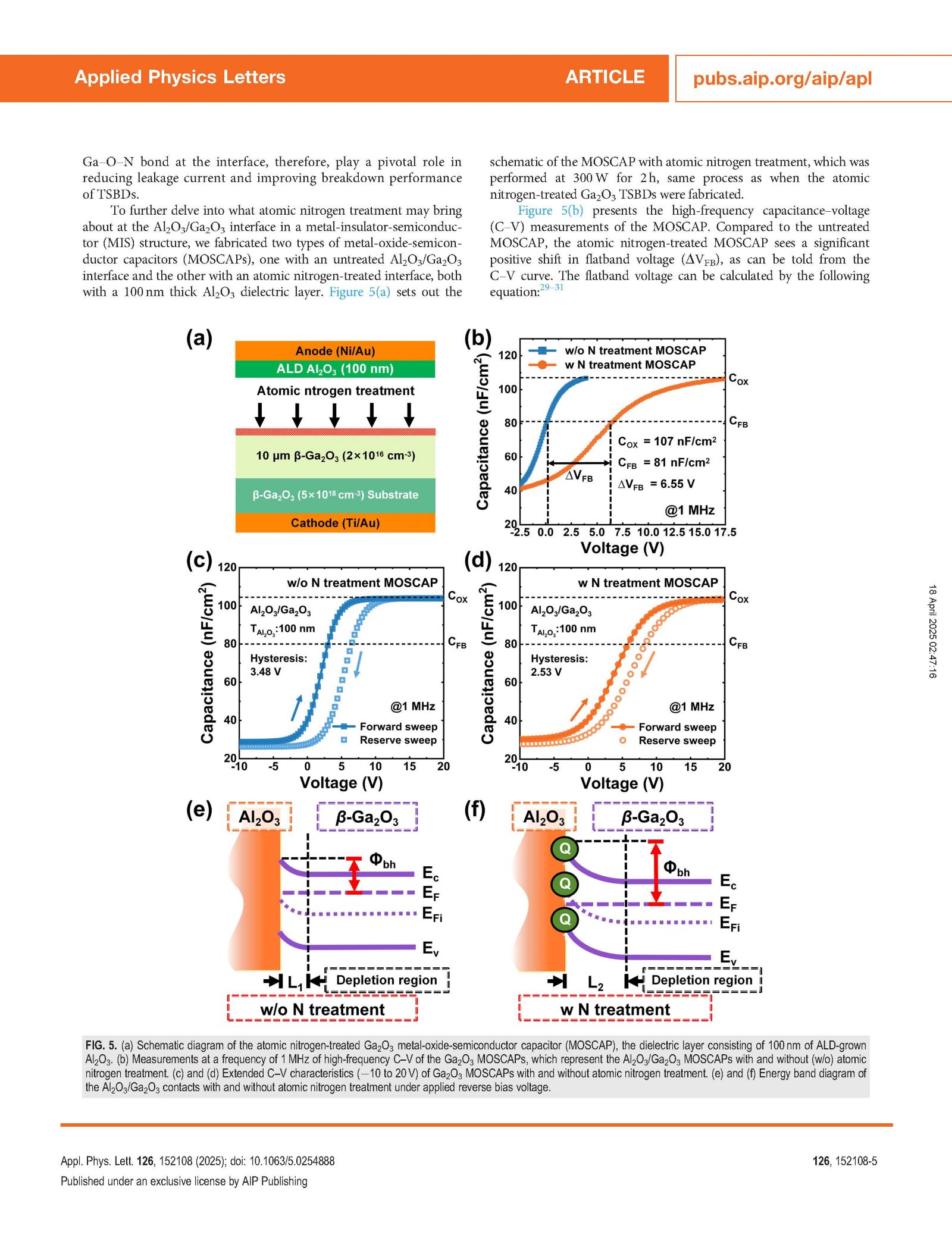
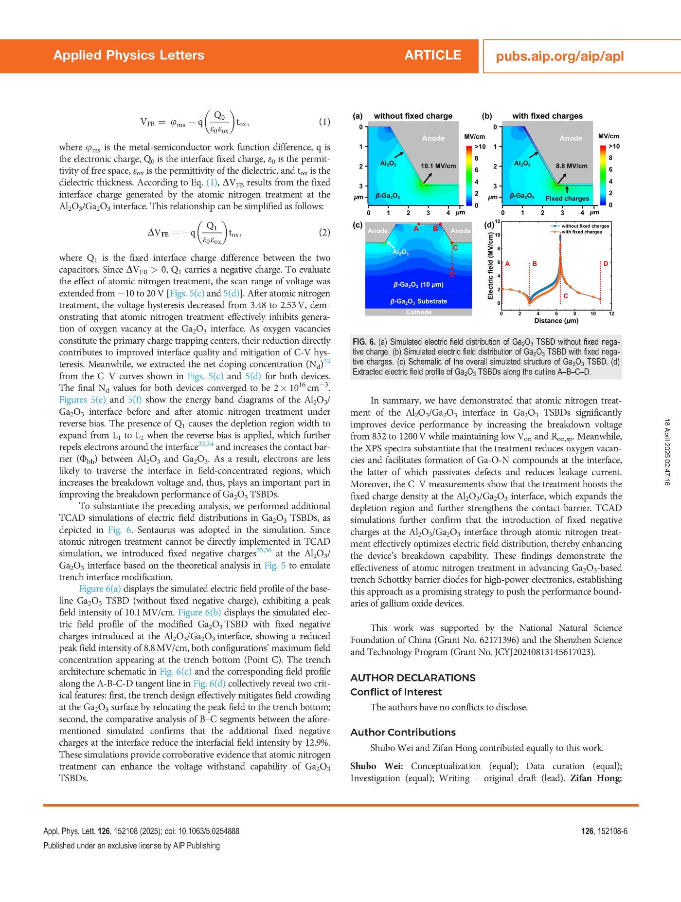
We demonstrate a significant improvement in the breakdown voltage of vertical β-Ga2O3 metal-insulator-semiconductor (MIS) trench Schottky barrier diodes (TSBDs) through atomic nitrogen treatment at the Al2O3/β-Ga2O3 interface. The treated TSBDs show a breakdown voltage increasing from 832 to 1200 V while maintaining a low turn-on voltage of 0.9 V and a low specific on-resistance of 12.1 mΩ cm2. As indicated by the x-ray photoelectron spectroscopy analysis, atomic nitrogen treatment reduces oxygen vacancies on the β-Ga2O3 surface and promotes the formation of ternary Ga–O–N compounds at the Al2O3/Ga2O3 interface. These compounds passivate ICP (Inductively Coupled Plasma)-induced defects on the Ga2O3 trench surface, reducing the leakage current in the Al2O3/Ga2O3 MIS TSBDs. Meanwhile, the atomic nitrogen treatment induces a positive shift in the flatband voltage of Ga2O3 MOS capacitors with Al2O3 dielectric, a sign of an increase in the fixed charge density (Q1) at the Al2O3/Ga2O3 interface, which expands the depletion region under reverse bias and strengthens the contact barrier. These findings testify to the fact that atomic nitrogen treatment effectively optimizes the trench MIS interface, promising to an effective strategy for high-performance Ga2O3-based Schottky barrier diodes.
Summary
In summary, we have demonstrated that atomic nitrogen treatment of the Al2O3/Ga2O3 interface in Ga2O3 TSBDs significantly improves device performance by increasing the breakdown voltage from 832 to 1200V while maintaining low Von and Ron,sp. Meanwhile, the XPS spectra substantiate that the treatment reduces oxygen vacancies and facilitates formation of Ga-O-N compounds at the interface, the latter of which passivates defects and reduces leakage current. Moreover, the C–V measurements show that the treatment boosts the fixed charge density at the Al2O3/Ga2O3 interface, which expands the depletion region and further strengthens the contact barrier. TCAD simulations further confirm that the introduction of fixed negative charges at the Al2O3/Ga2O3 interface through atomic nitrogen treatment effectively optimizes electric field distribution, thereby enhancing the device’s breakdown capability. These findings demonstrate the effectiveness of atomic nitrogen treatment in advancing Ga2O3-based trench Schottky barrier diodes for high-power electronics, establishing this approach as a promising strategy to push the performance boundaries of gallium oxide devices.
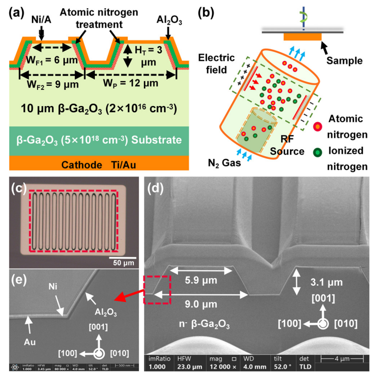
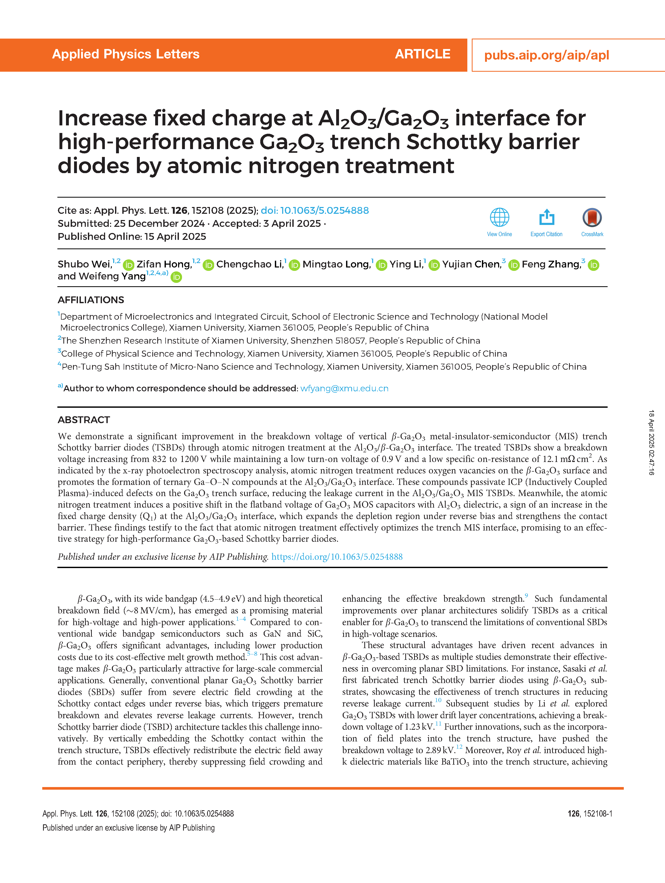
FIG. 1. (a) Schematic cross section of the atomic nitrogen-treated Ga2O3 TSBD. (b) Schematic illustration of the atomic nitrogen source interface treatment process in which high-energy ionized nitrogen was filtered by an electric field (i.e., plasma confinement plate), and nitrogen atoms were enabled to reach and interact with the sample surface. (c) Top view of the Ga2O3 TSBD captured under an optical microscope, and the red dashed box indicates the area used to calculate current density. (d) SEM image of the Ga2O3 TSBD, clearly showing the trench structure and the sloped trapezoidal interface formed by etching. (e) High-magnification SEM image of a specific area in (d).

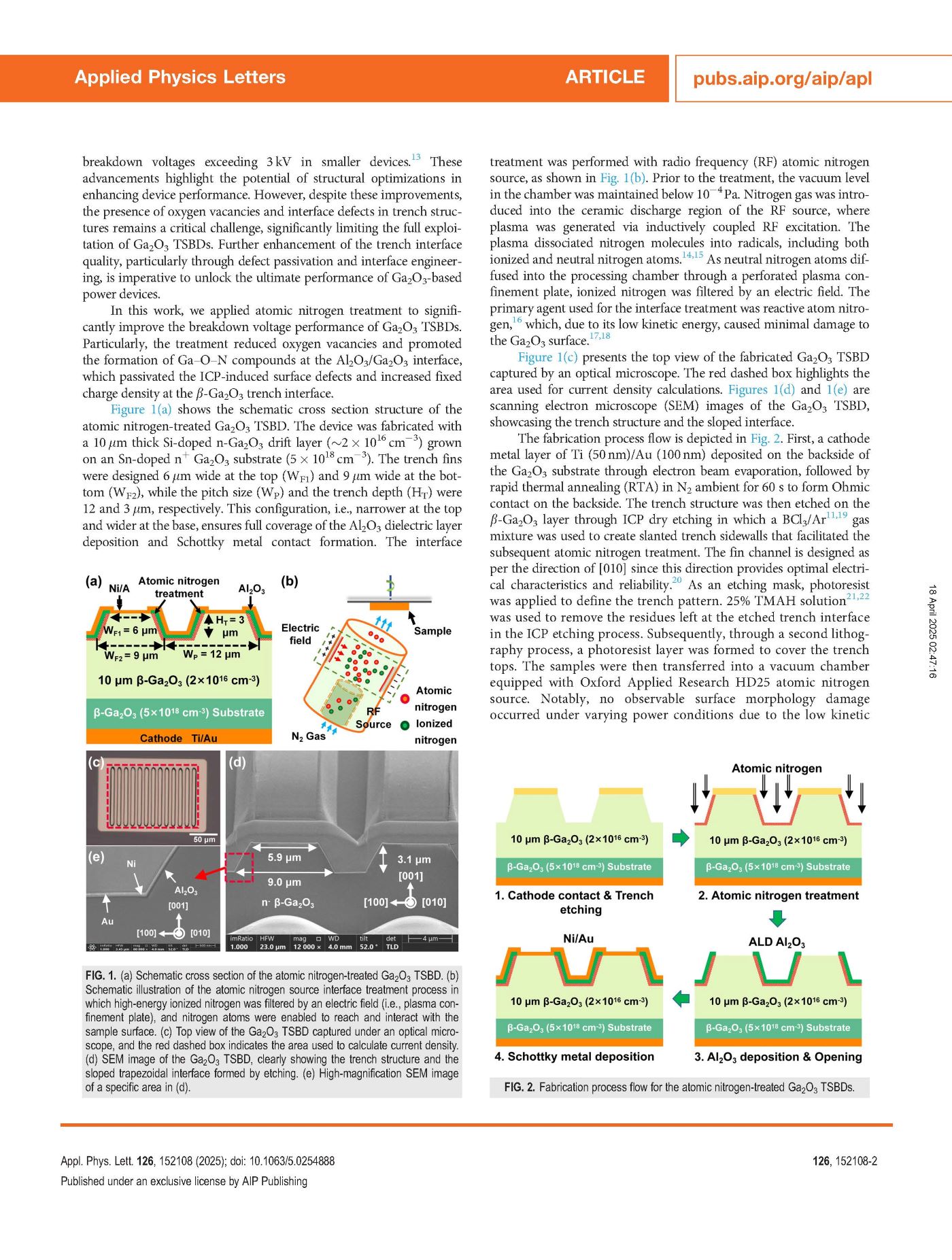
FIG. 2. Fabrication process flow for the atomic nitrogen-treated Ga2O3 TSBDs.
DOI:
doi.org/10.1063/5.0254888