Paper Sharing
【Member Papers】Research Paper from Prof. Bingsheng Li’s MOCVD Research Group in Academician Yichun Liu’s Team at Northeast Normal University --- High-Performance β-Ga₂O₃/GaN Ultraviolet Detector Achieved via GaON Nucleation Layer Introduction in Reversed Substitution Growth Method
日期:2025-04-28阅读:848
Researchers at the State Key Laboratory of Integrated Optoelectronics, Northeast Normal University, published a research paper entitled Enhanced performance UV photodetectors based on the β-Ga2O3/GaN photodiode of the reversed substitution growth with introduction nucleation layer of GaON by oxygen plasma treatment in the journal Materials Today Physics.
Project Support
This work was supported by the National Natural Science Foundation of China under Grant 62274027 and 62404039, the Open Research Fund of Songshan Lake Materials Laboratory (2023SLABFK03) and the funding from Jilin Province (NO. 20220502002GH), the Postdoctoral Fellowship Program of CPSF (GZC20230416), the Fundamental Research Funds for the Central Universities (2412024QD010).
Background
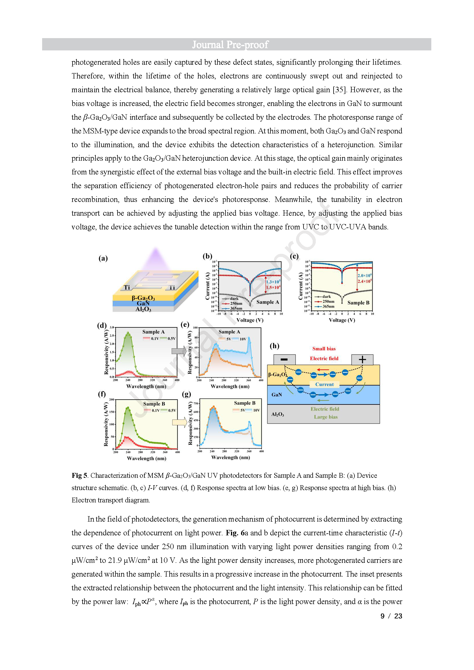
β-Ga2O3 demonstrates potential as a UV photodetector material due to its high absorption coefficient and efficient photon absorption in UV spectrum. To enhance photoelectric conversion efficiency, the construction of heterojunctions is a widely adopted strategy to modulate charge carriers while promoting their separation and transport. The β-Ga2O3/GaN heterojunction has garnered considerable attention owing to its relatively small lattice mismatch. Conventional epitaxial n-β-Ga2O3/p-GaN heterojunctions suffer from interfacial barriers that impede carrier transport and reduce detection efficiency, while the reverse substitution method is prone to causing surface thermal damage due to excessively rapid oxidation rates at high temperatures. This study proposed an oxygen plasma treatment (OPT)-assisted reverse substitution method to pre-form a GaON nucleation layer on GaN surfaces, and systematically investigated the influence of the GaON layer on subsequent oxidation behavior and interfacial charge transfer dynamics.
Article Abstract
A high-performance β-Ga2O3/GaN ultraviolet photodetector with bias-tunable spectral response (the UVC band to the UVA-UVC band) is demonstrated. The device is fabricated via a new route of reverse substitution growth, combined with oxygen plasma treatment (OPT) to introduce a GaON nucleation layer for the β-Ga2O3 synthesis on the GaN surface. The effects of the nucleation layer on the subsequent transformation from GaN to β-Ga2O3 at high temperature under oxygen ambience were analyzed in detail. X-ray diffraction (XRD) confirmed that (− 201) preferred oriented monoclinic phase β-Ga2O3 with narrow linewidths has been formed. Both oxygen vacancies (VO) on the surface and the root mean square (RMS) of the surface roughness of β-Ga2O3 treated with OPT are reduced, as confirmed by X-ray photoelectron spectroscopy (XPS) and atomic force microscopy (AFM), resulting in better interfacial contact with the electrodes. Meanwhile, the increase in internal VO enhanced the conductivity of the material, thereby improving the photoelectric response performance. The metal - semiconductor-metal (MSM) device achieved ultra-high detection capabilities (responsivity = 653 A/W, detectivity = 2.9 × 10¹⁵ Jones) and response spectrum switches between solar-blind narrow band and broad UVA-UVC band by varying the applied bias. The transient response time was on the millisecond scale. In the vertical-type β-Ga2O3/GaN photodiode, the responsivity and detectivity of the photodetector reached 2.1 A/W and 7.2 × 10¹³ Jones with a fast transient response time (rise time = 0.24 ms, decay time = 17.1 ms) under a bias voltage of − 10 V.
Innovation Point
·Using the reverse substitution method, residual nitrogen (acting as an acceptor) led to a lower Fermi level in the resulting Ga2O3 compared to GaN. This altered the transport direction of photogenerated carriers and helped avoid interface barriers caused by band offset.
·The OPT-assisted reverse substitution method introduced a GaON nucleation layer prior to thermal oxidation, effectively reducing the oxidation rate.
·This approach suppressed oxygen vacancies in β-Ga2O3, minimized surface defects, and enhanced the material’s electrical conductivity.
·Tunable detection from the UVC band to the UVA-UVC band was achieved by controlling the applied bias voltage.
Conclusion
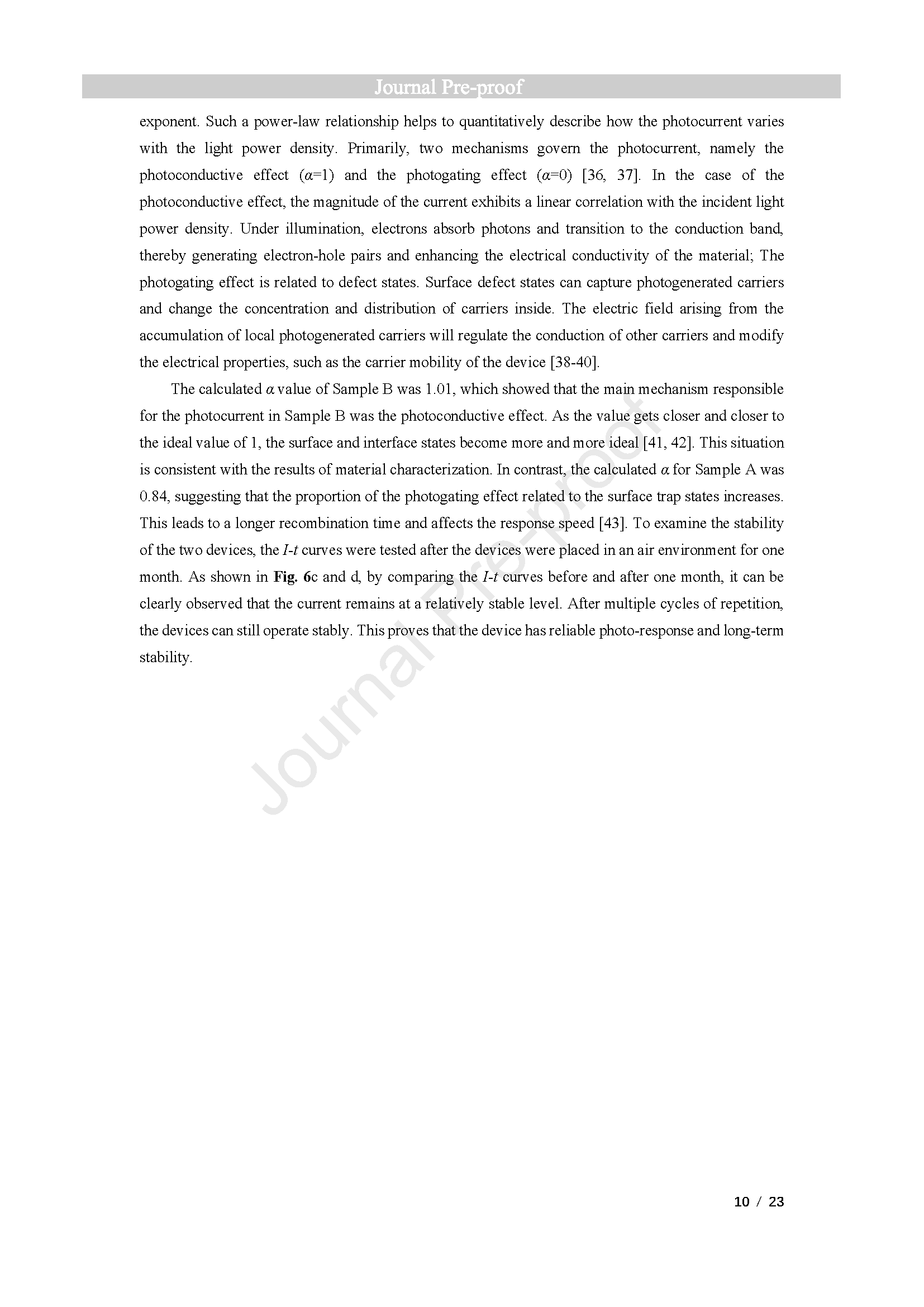
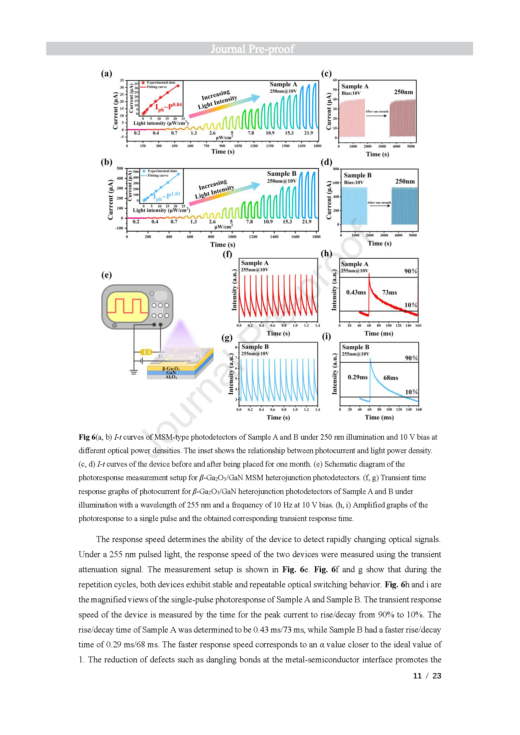
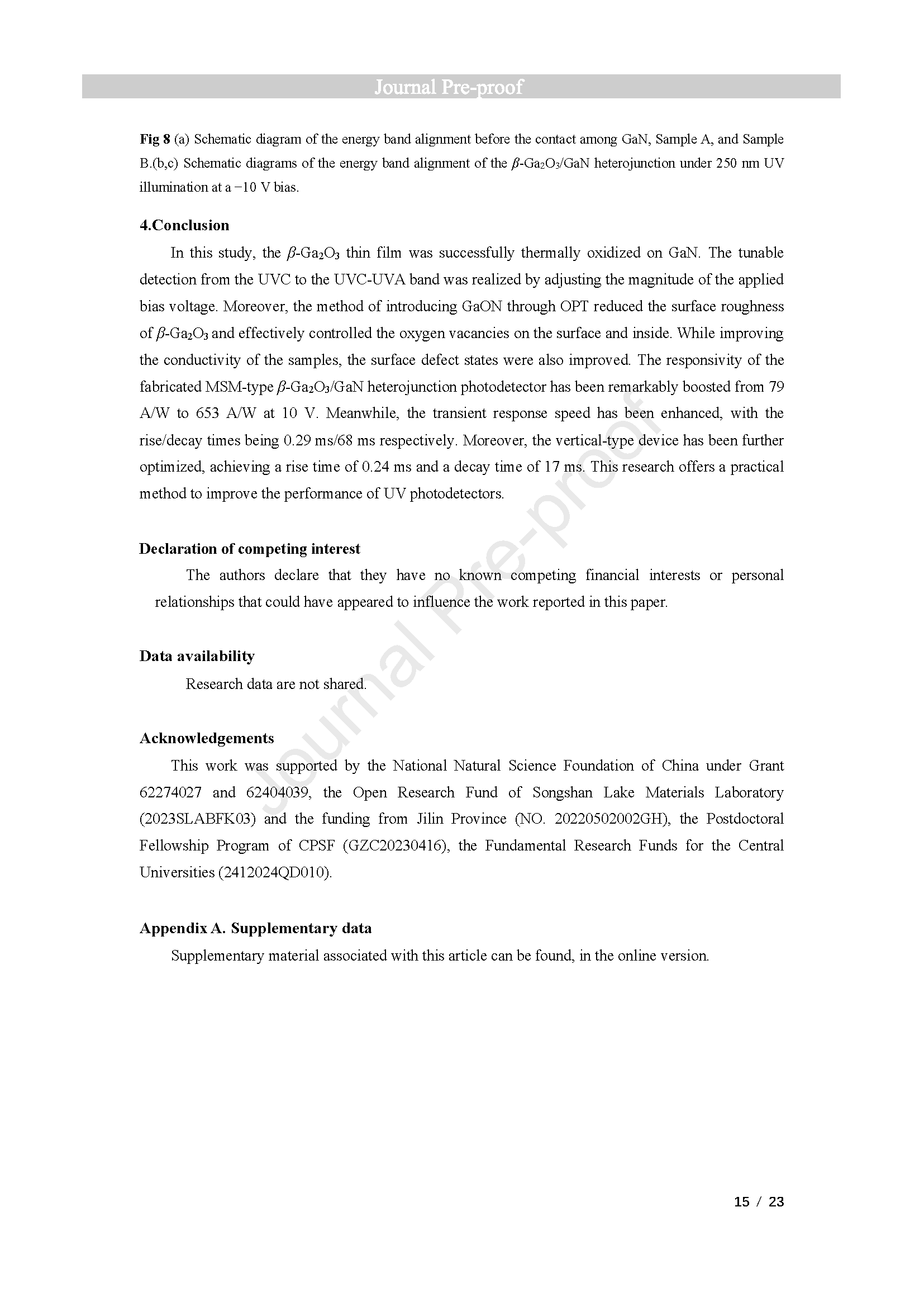
In this study, the β-Ga2O3 thin film was successfully thermally oxidized on GaN. The tunable detection from the UVC to the UVC-UVA band was realized by adjusting the magnitude of the applied bias voltage. Moreover, the method of introducing GaON through OPT reduced the surface roughness of β-Ga2O3 and effectively controlled the oxygen vacancies on the surface and inside. While improving the conductivity of the samples, the surface defect states were also improved. The responsivity of the fabricated MSM-type β-Ga2O3 /GaN heterojunction photodetector has been remarkably boosted from 79 A/W to 653 A/W at 10 V. Meanwhile, the transient response speed has been enhanced, with the rise/decay times being 0.29 ms/68 ms respectively. Moreover, the vertical-type device has been further optimized, achieving a rise time of 0.24 ms and a decay time of 17 ms. This research offers a practical method to improve the performance of UV photodetectors.
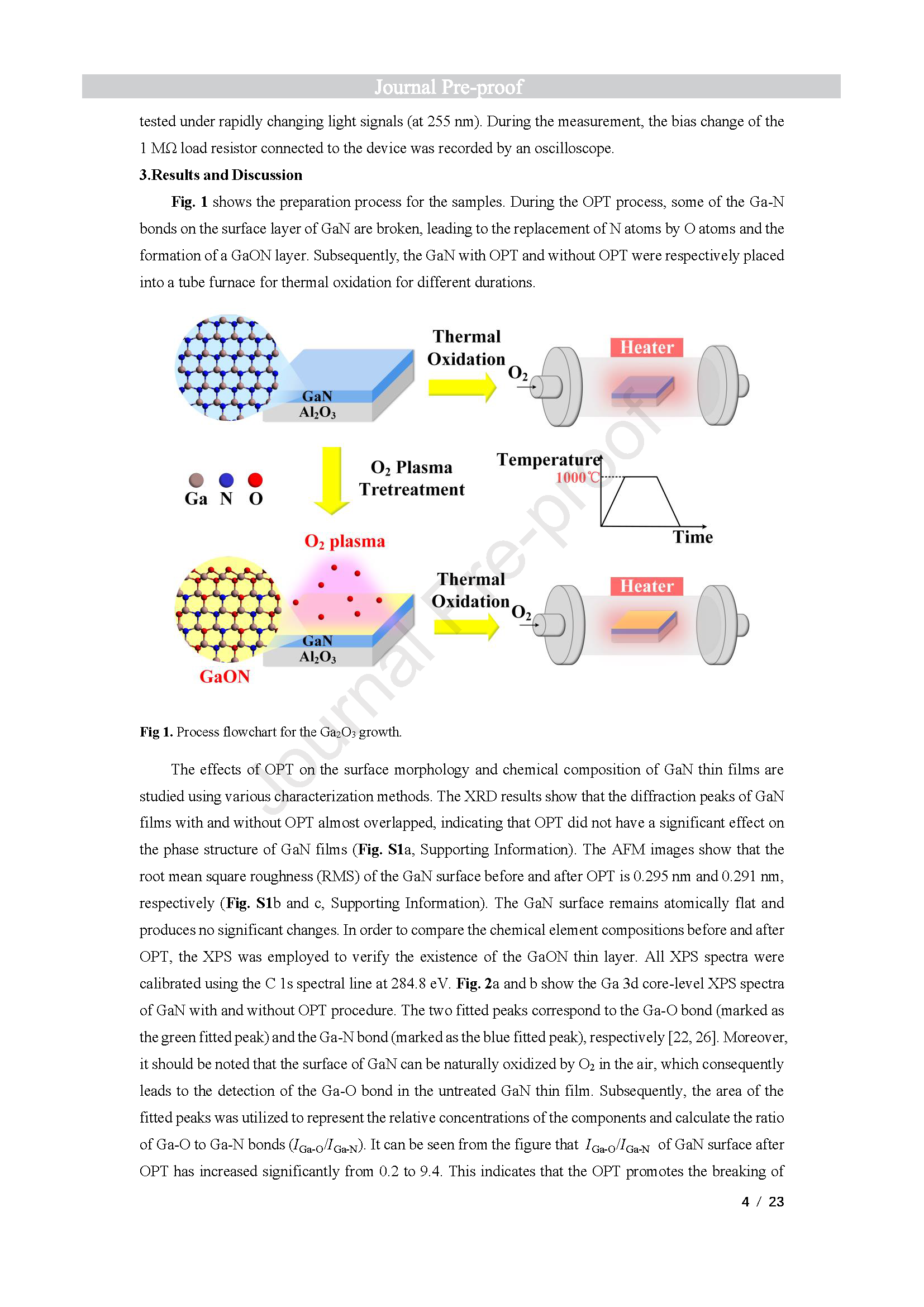
Graphic Abstract
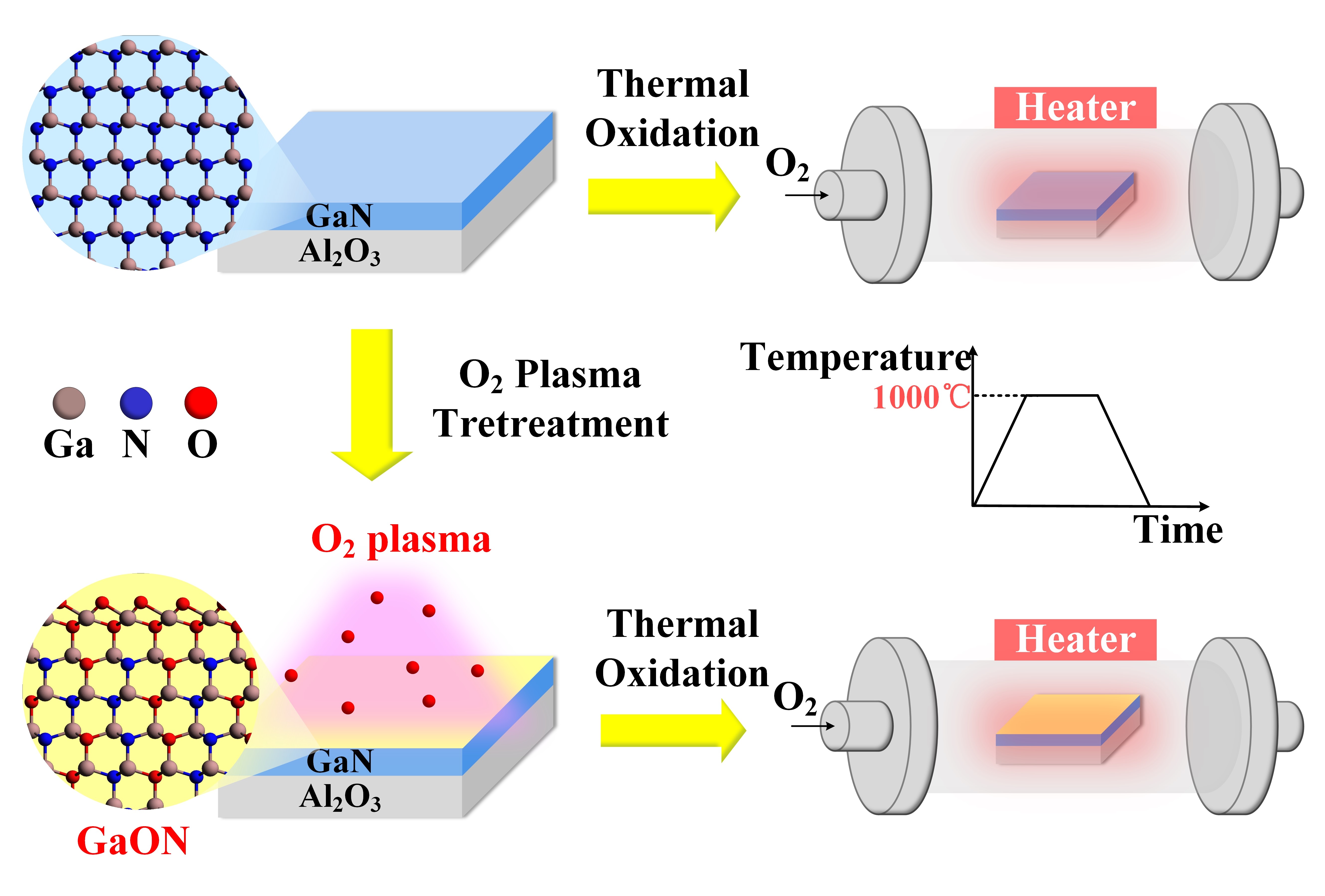
Fig. 1. Process flowchart for the Ga2O3 growth.
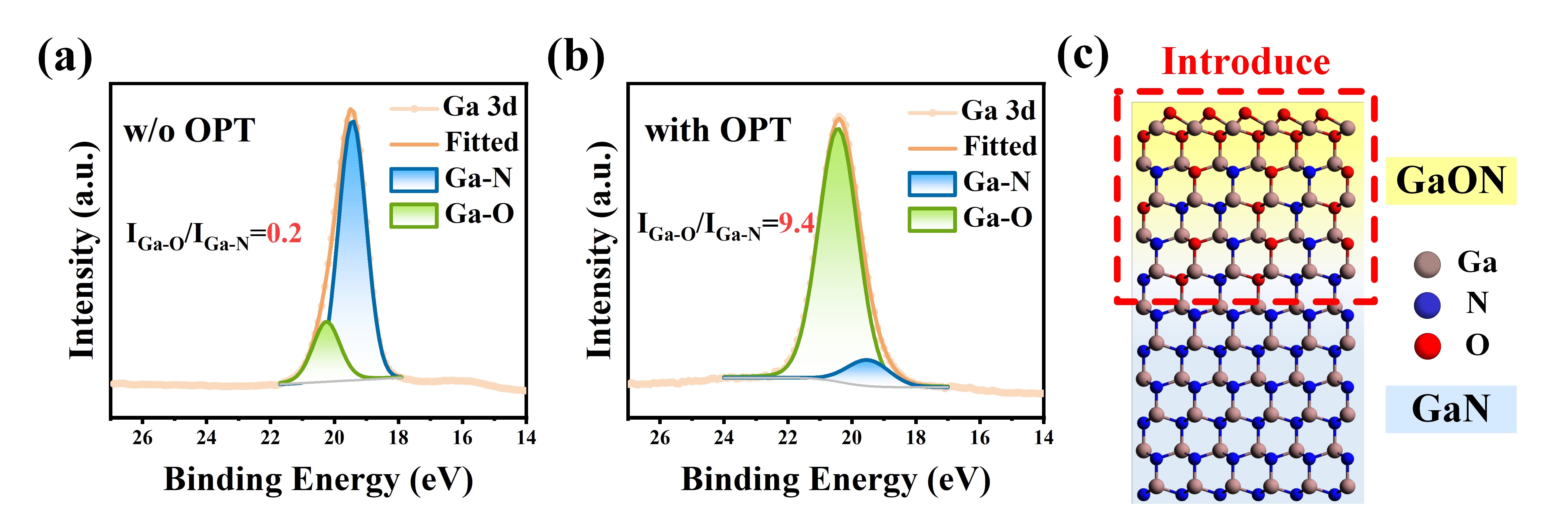
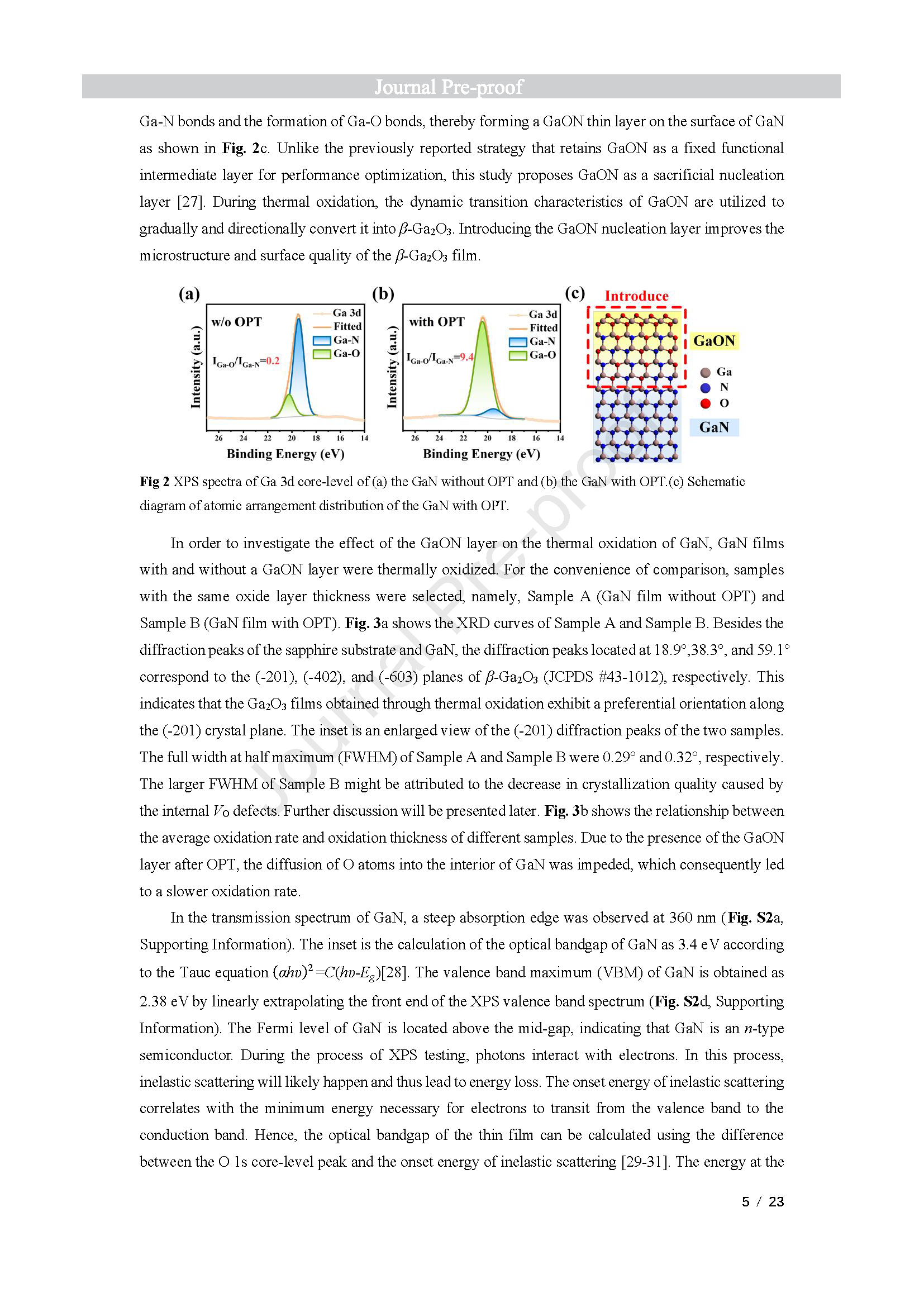
Fig. 2. XPS spectra of Ga 3d core-level of (a) the GaN without OPT and (b) the GaN with OPT.(c) Schematic diagram of atomic arrangement distribution of the GaN with OPT
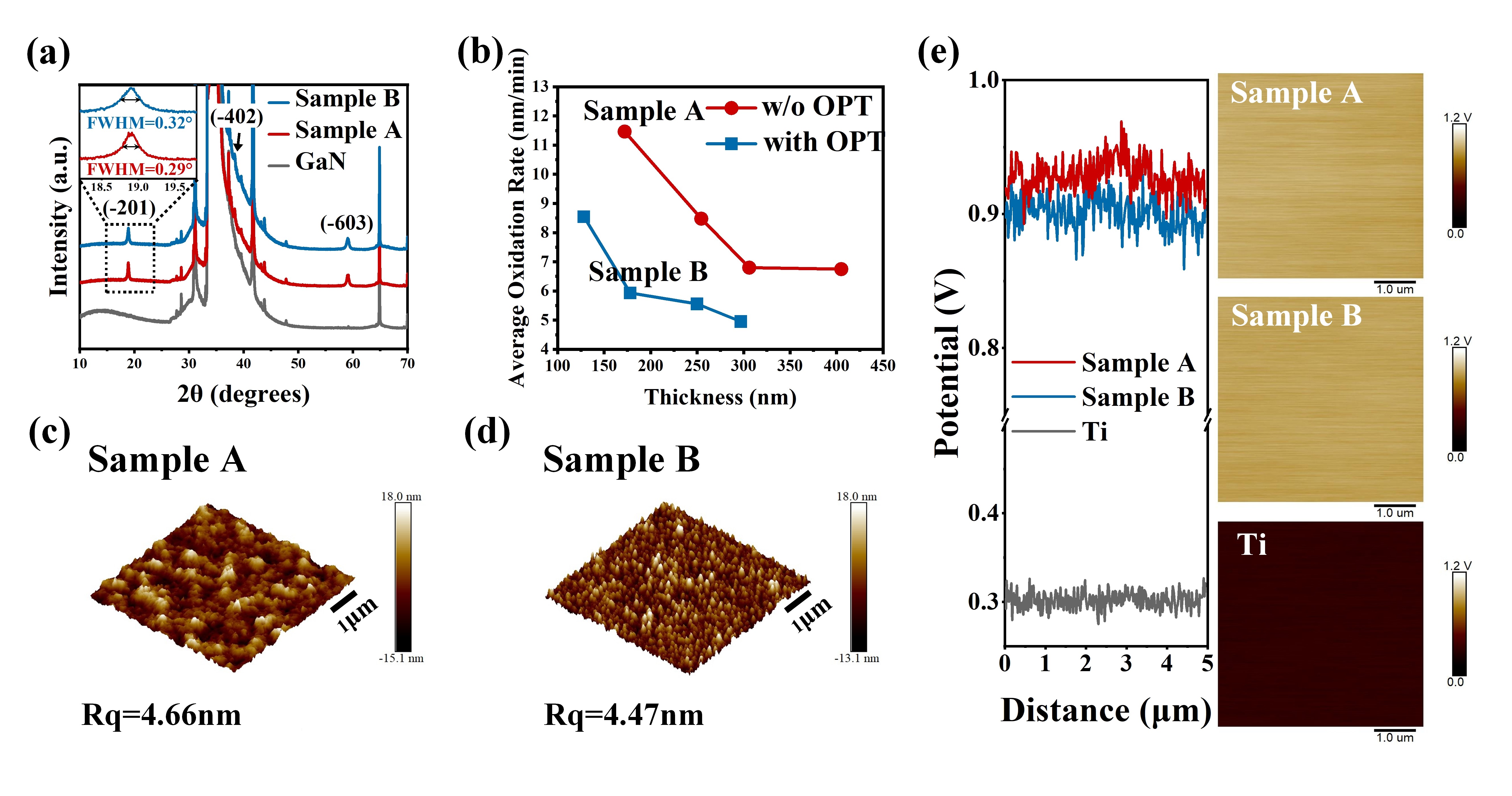
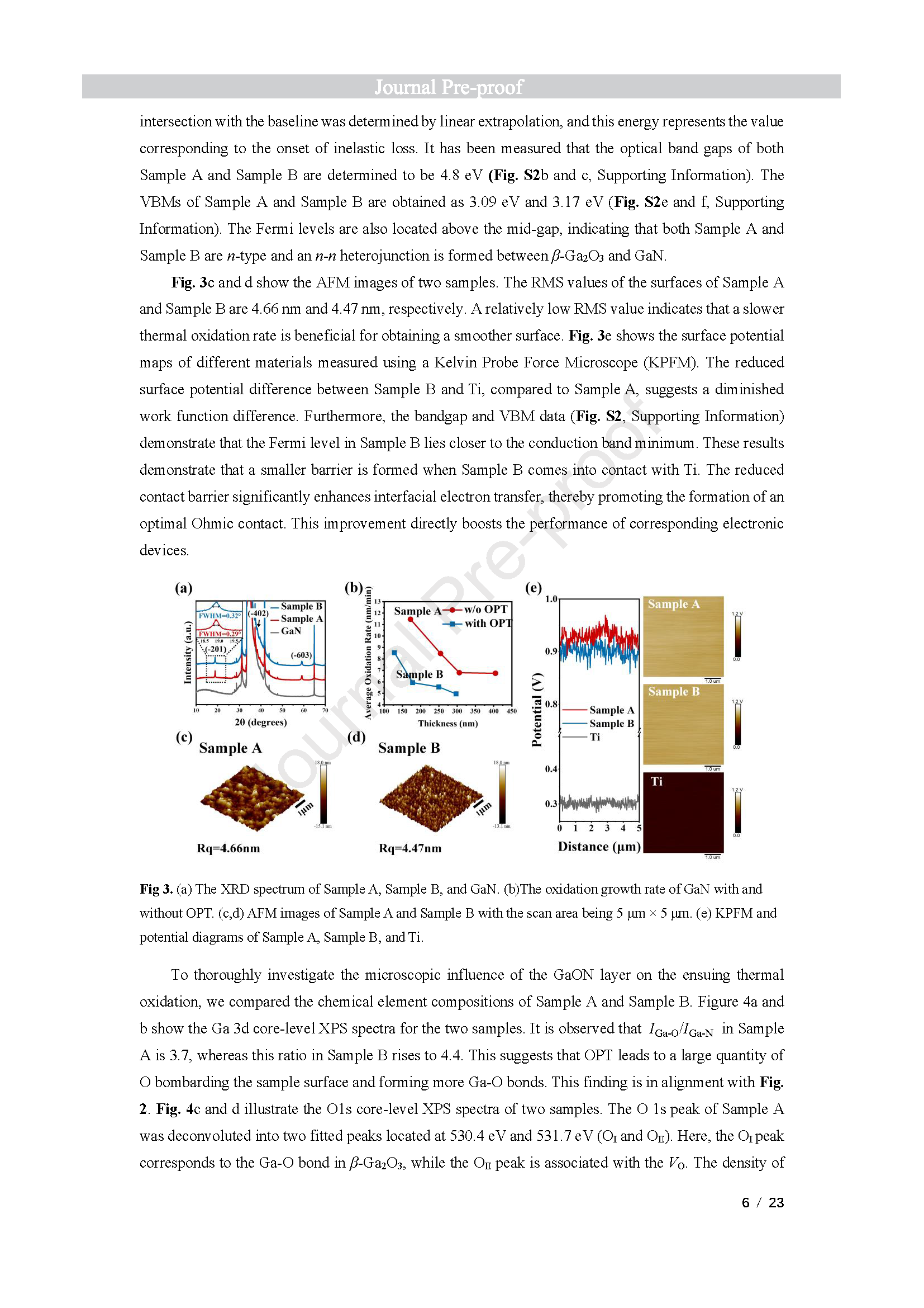
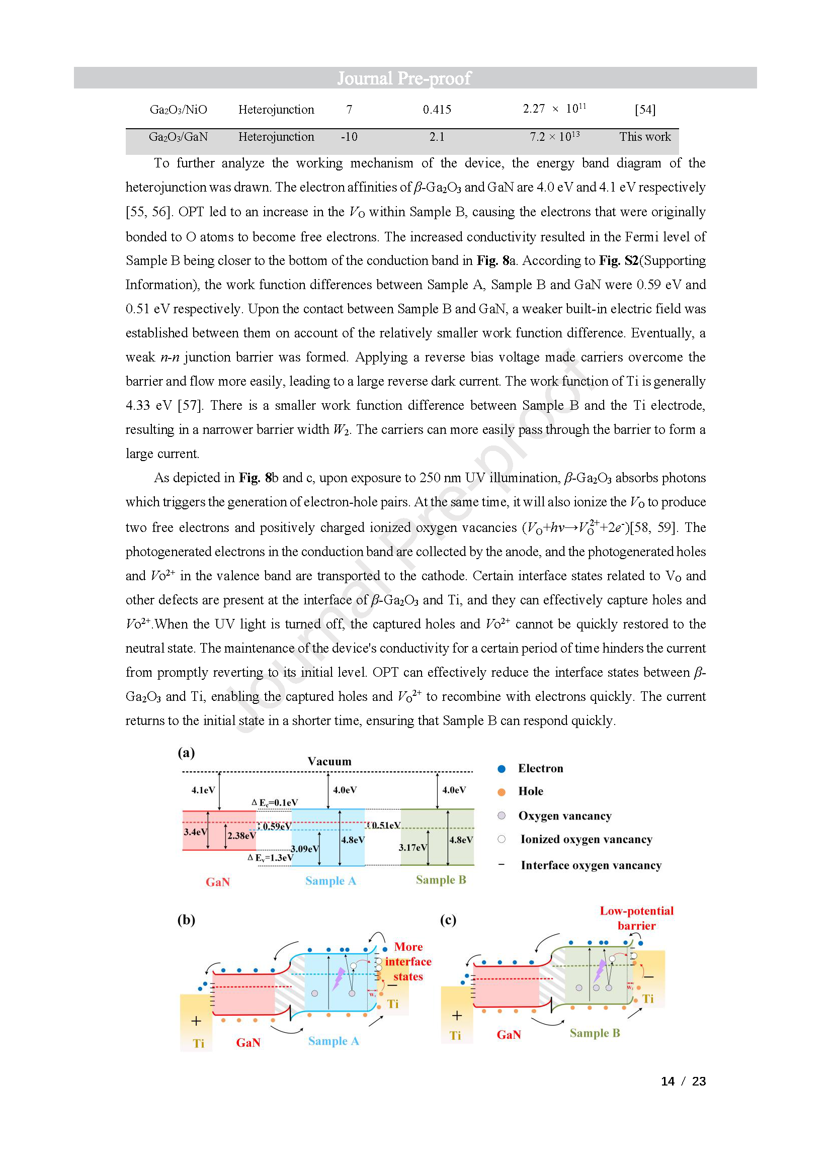
Fig. 3. (a) The XRD spectrum of Sample A (Ga2O3 from GaN oxidation without OPT), Sample B (Ga2O3 from GaN oxidation with OPT), and GaN. (b)The oxidation growth rate of GaN with and without OPT. (c,d) AFM images of Sample A and Sample B with the scan area being 5 μm × 5 μm. (e) KPFM and potential diagrams of Sample A, Sample B, and Ti.
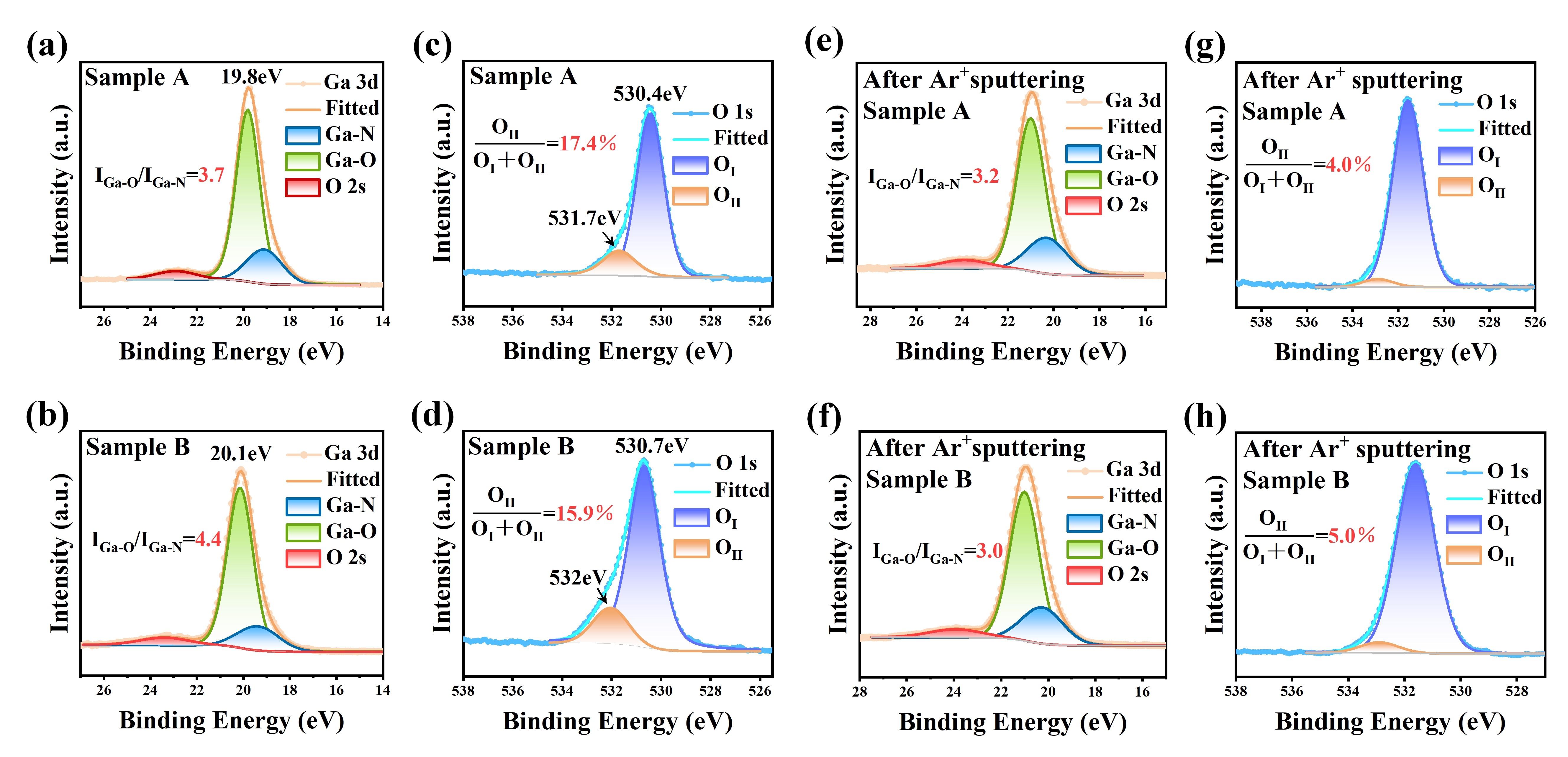
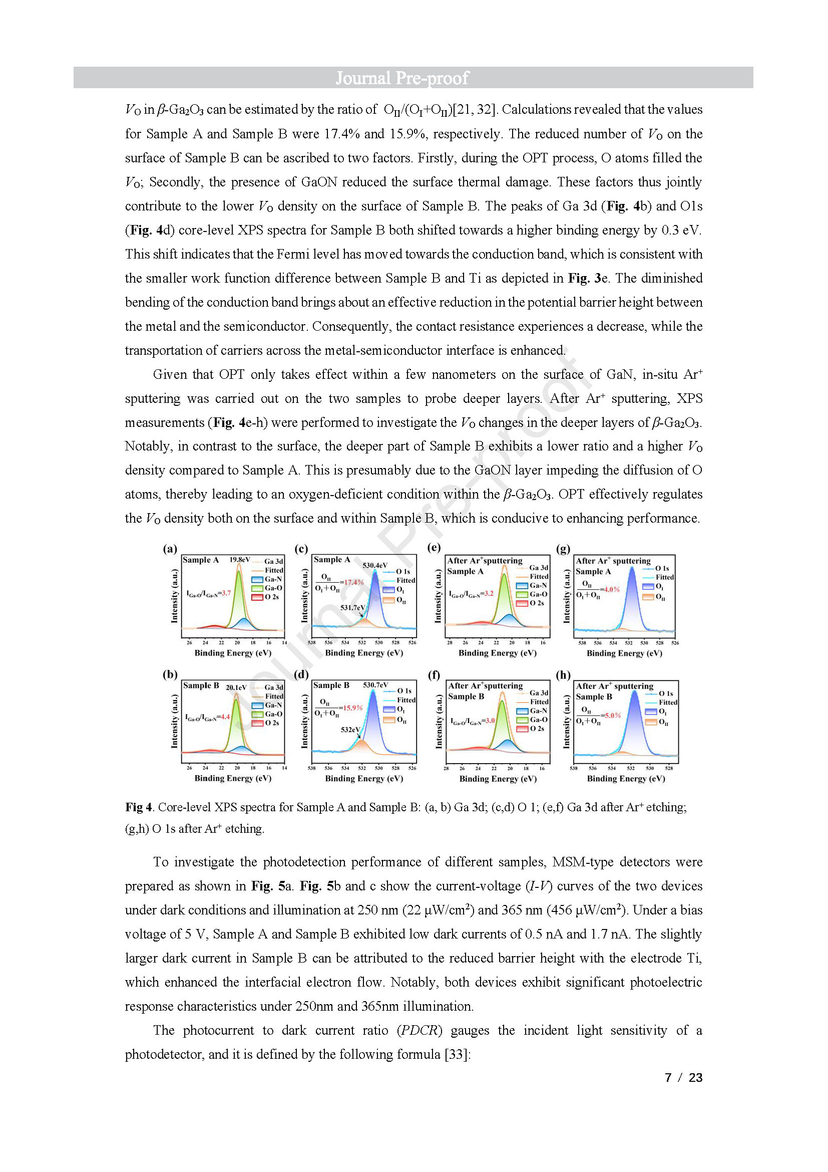
Fig. 4. Core-level XPS spectra for Sample A and Sample B: (a, b) Ga 3d; (c,d) O 1s; (e,f) Ga 3d after Ar+ etching; (g,h) O 1s after Ar+ etching.
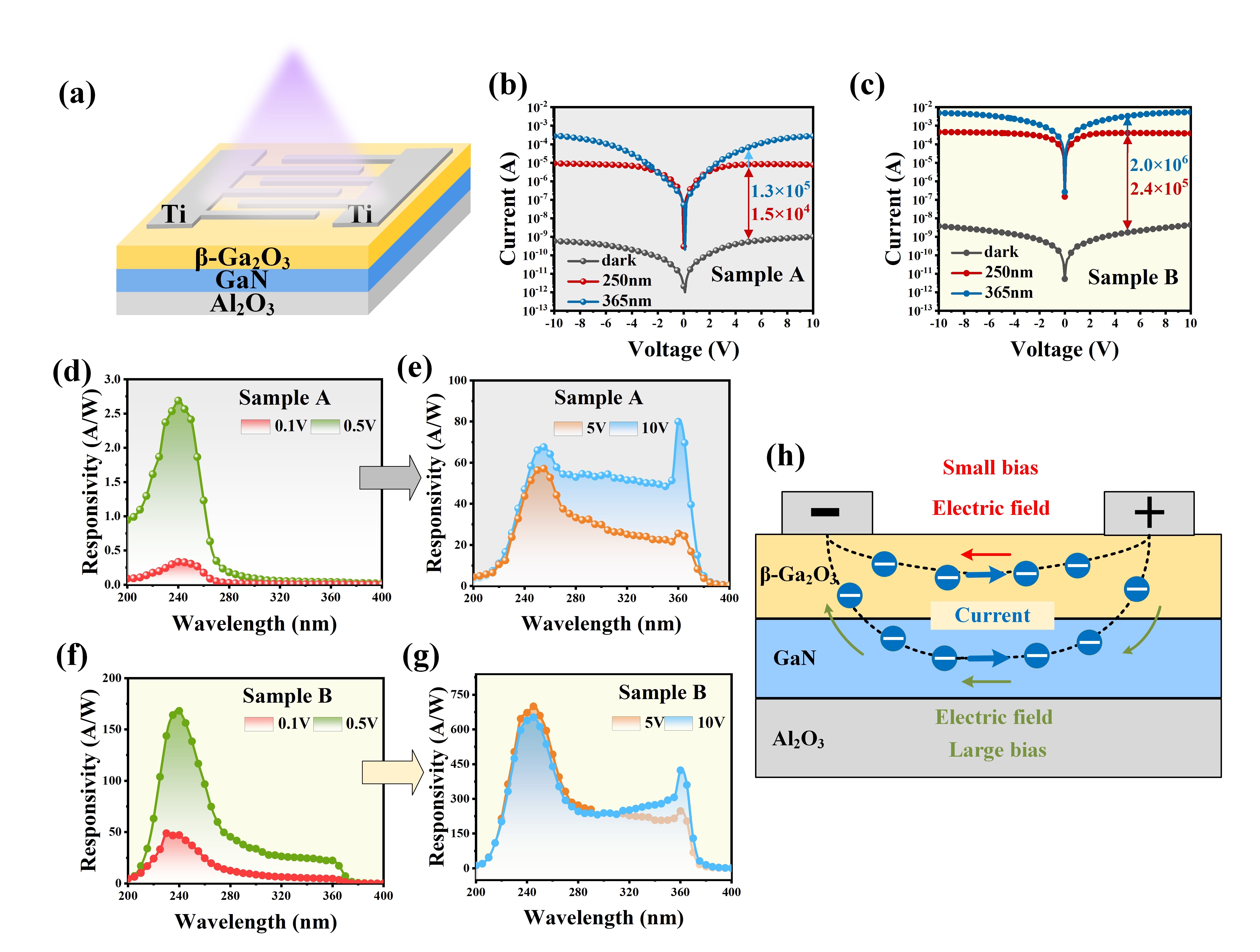
Fig. 5. Characterization of MSM β-Ga2O3/GaN UV photodetectors for Sample A and Sample B: (a) Device structure schematic. (b, c) I-V curves. (d, f) Response spectra at low bias. (e, g) Response spectra at high bias. (h) Electron transport diagram.
DOI:
doi.org/10.1016/j.mtphys.2025.101729