Paper Sharing
【Domestic Papers】Fuzhou University --- Insight into the High Hole Concentration of p-Type Ga₂O₃ via In Situ Nitrogen Doping
日期:2025-04-29阅读:1004
Researchers from the Fuzhou University have published a dissertation titled "Insight into the High Hole Concentration of p-Type Ga2O3 via In Situ Nitrogen Doping" in The Journal of Physical Chemistry Letters.
Project Support
This work was financially supported by the National Natural Science Foundation of China (Grant No. 62204270), the Major Science and Technology Special Project of Fujian Province (Grant No. 2022HZ027006), the Fujian Provincial Natural Science Foundation General Program (Grant No. 2024J01251), the Fujian Provincial Science and Technology Program Project (Grant No. 2022I0006), and the Major Science and Technology Special Project of Quanzhou Municipality (Grant No. 2022GZ7). The authors also thank Fujia Co. Ltd. for help in the growth of epitaxial films.
Background
Gallium oxide (Ga2O3) holds significant potential for applications in the field of high-voltage, low-loss power electronics due to its ultra-wide bandgap of 4.95 eV and high Baliga figure of merit exceeding 3000. However, the lack of an effective p-type doping method, crucial for forming hole conduction paths to achieve avalanche characteristics in high-voltage devices, is widely recognized as a critical bottleneck for the further application of Ga2O3. Although p-type nickel oxide (NiO) has partially alleviated the issue of missing hole conductivity, a p-type conduction mechanism induced by nickel vacancies at room temperature (RT) is susceptible to significant reductions in hole concentration and severe device degradation under frequent switching or higher voltage/ temperature conditions.
Abstract
The unclear p-type conduction mechanism and lack of reliable p-type Ga2O3 severely hinder Ga2O3-based high-voltage electronics. Here, we demonstrate in situ nitrogen (N) doping via metal–organic chemical vapor deposition homoepitaxy using N2O as oxygen source and acceptor dopant. Structural and compositional analyses confirm efficient N incorporation (favored by N–Ga bonding) compensating residual Si/H donors without compromising crystallinity. The Ga2O3:N epilayers achieve excellent p-type performance: 1.04 × 1018 cm–3 hole concentration, 0.47 cm2 V–1 s–1 mobility at room temperature, and 0.168 eV activation energy. A completely new insight into the p-type conduction mechanism in Ga2O3 is introduced, focusing on the crystallographic visualization of acceptors (N2–) and holes (O–), as well as the hole excitation process. It is suggested that careful suppression of the donor compensation effect and precise control of the N chemical potential, which leads to the fabrication of trace O– species solid-dissolved within Ga2O3, are essential for achieving high-hole-concentration p-type conduction in oxides.
Summary
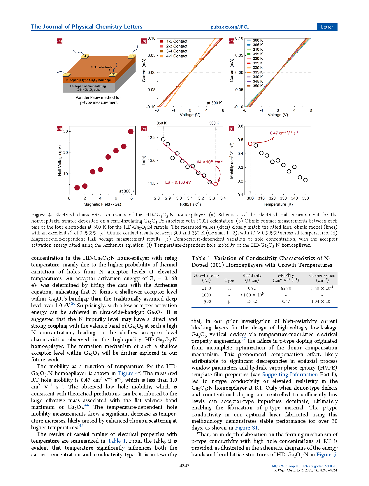
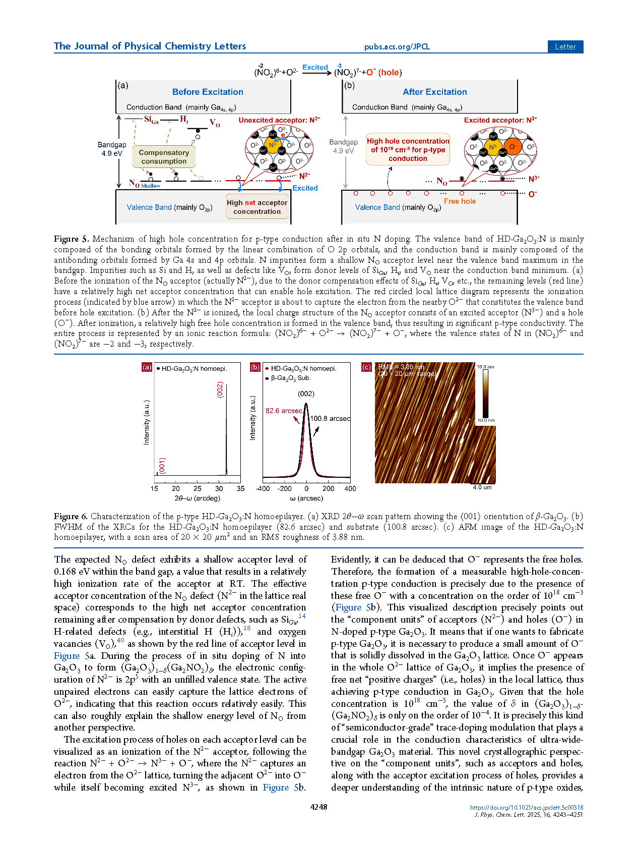
In summary, we propose a strategy for in situ N doping through MOCVD homoepitaxy to achieve p-type Ga2O3. By leveraging the high bond energy of the N−Ga bond, which is comparable to that of the O−Ga bond, and maintaining 2D step-flow growth, we successfully tuned the electrical properties of Ga2O3:N from n-type to p-type by modulating the growth temperature. For the first time, we achieved a high RT hole concentration of 1.04×1018 cm−3 and a hole mobility of 0.47 cm2 V−1 s−1 , accompanied by a low acceptor activation energy of 0.168 eV. Our results demonstrate that N acceptor impurities can be incorporated into the Ga2O3 lattice at high concentrations and substitute O sites at high temperature. Furthermore, a completely new crystallographic insight into the p-type conduction mechanism in Ga2O3:N is presented, revealing the nature of acceptors (N2−) and holes (O−) in ptype conductivity oxides, along with the chemical reaction process N2− + O2− → N3− + O−) underlying the activation of shallow-level acceptors. It is suggested that, for successful semiconductor-grade p-type Ga2O3 fabrication, the donor compensation effect induced by defects or unintentional doping impurities must be strictly controlled to sufficiently low levels, enabling acceptor-type NO defects to dominate, and thereby allowing a small amount of O− species to be stably solid-solved within the Ga2O3 lattice. This work presents a potential pathway for the application of p-type Ga2O3 in high-voltage power devices.
Graphic Examples
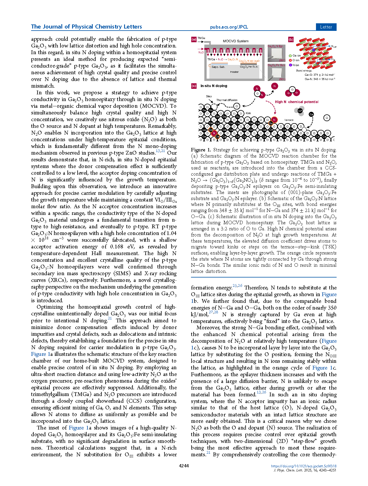
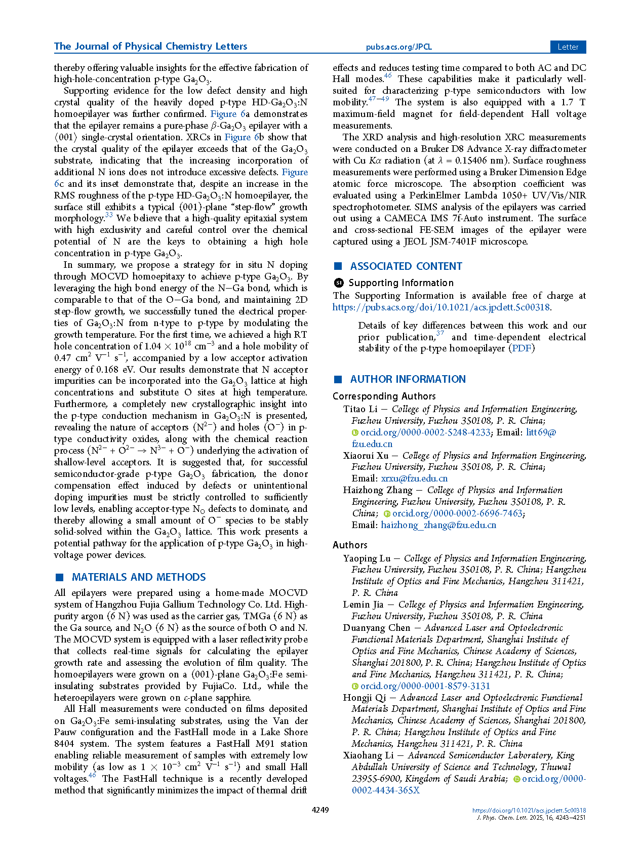
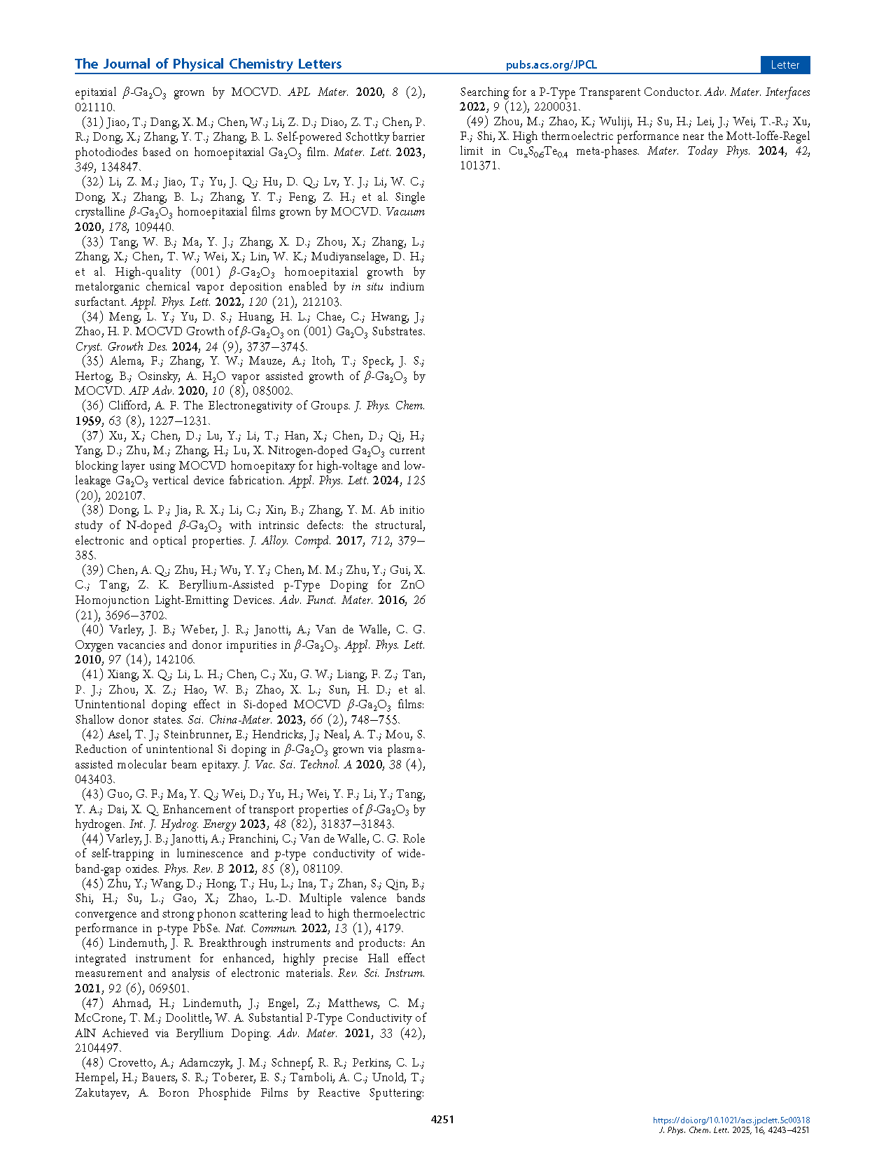
Figure 1. Strategy for achieving p-type Ga2O3 via in situ N doping. (a) Schematic diagram of the MOCVD reaction chamber for the fabrication of p-type Ga2O3 based on homoepitaxy. TMGa and N2O, used as reactants, are introduced into the chamber from a CCS-configured gas distribution plate and undergo reactions of TMGa + N2O → (Ga2O3)1-δ(Ga2NO2)δ (δ ranges from 10−6 to 10−3 ), finally depositing p-type Ga2O3:N epilayers on Ga2O3:Fe semi-insulating substrates. The insets are photographs of (001)-plane Ga2O3:Fe substrate and Ga2O3:N epilayer. (b) Schematic of the Ga2O3:N lattice where N primarily substitutes at the OIII sites, with bond energies ranging from 348 ± 35 kJ mol−1 for N−Ga and 374 ± 21 kJ mol−1 for O−Ga. (c) Schematic illustration of in situ N doping into the Ga2O3 lattice during MOCVD homoepitaxy. The Ga2O3 host lattice is arranged in a 3:2 ratio of O to Ga. High N chemical potential arises from the decomposition of N2O at high growth temperatures. At these temperatures, the elevated diffusion coefficient drives atoms to migrate toward kinks or steps on the terrace−step−kink (TSK) surfaces, enabling layer-by-layer growth. The orange circle represents the state where N atoms are tightly connected by Ga through strong N−Ga bonds. The similar ionic radii of N and O result in minimal lattice distortion.
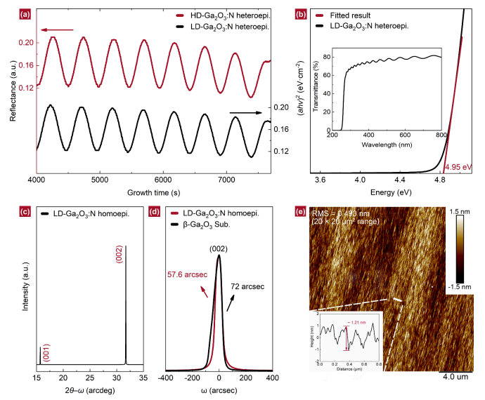
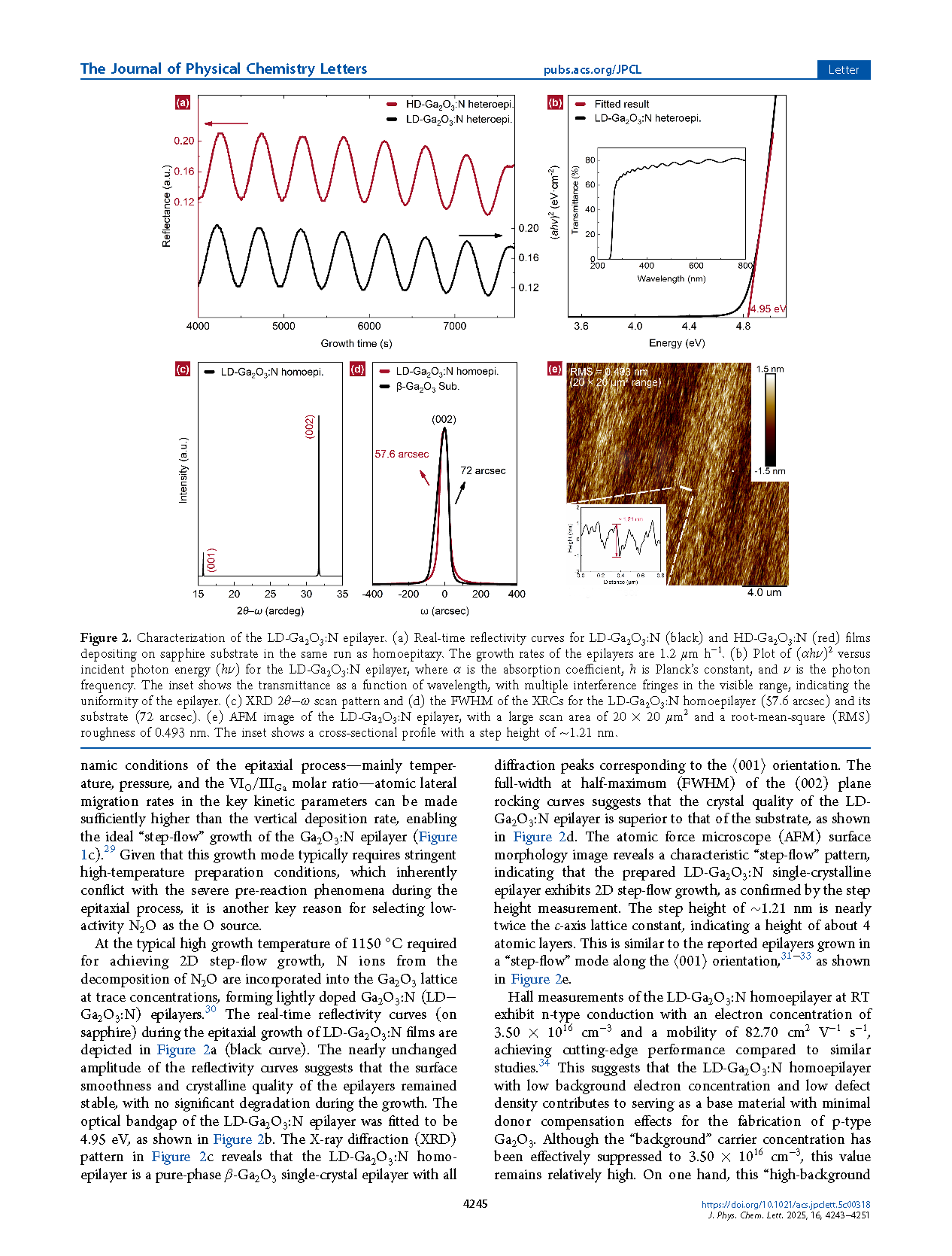
Figure 2. Characterization of the LD-Ga2O3:N epilayer. (a) Real-time reflectivity curves for LD-Ga2O3:N (black) and HD-Ga2O3:N (red) films depositing on sapphire substrate in the same run as homoepitaxy. The growth rates of the epilayers are 1.2 μm h−1 . (b) Plot of (αhν)2 versus incident photon energy (hν) for the LD-Ga2O3:N epilayer, where α is the absorption coefficient, h is Planck’s constant, and ν is the photon frequency. The inset shows the transmittance as a function of wavelength, with multiple interference fringes in the visible range, indicating the uniformity of the epilayer. (c) XRD 2θ−ω scan pattern and (d) the FWHM of the XRCs for the LD-Ga2O3:N homoepilayer (57.6 arcsec) and its substrate (72 arcsec). (e) AFM image of the LD-Ga2O3:N epilayer, with a large scan area of 20 × 20 μm2 and a root-mean-square (RMS) roughness of 0.493 nm. The inset shows a cross-sectional profile with a step height of ∼1.21 nm.
DOI:
doi.org/10.1021/acs.jpclett.5c00318