Paper Sharing
【International Papers】Breakdown-induced directional cracking in kilovolt-class β-Ga₂O₃ (001) vertical trench Schottky barrier diodes
日期:2025-05-06阅读:822
Researchers from the University of Bristol have published a dissertation titled "Breakdown-induced directional cracking in kilovolt-class β-Ga2O3 (001) vertical trench Schottky barrier diodes" in Applied Physics Letters.
Corresponding Author Introduction

Martin H H Kuball教授
Professor Martin H H Kuball is Royal Academy of Engineering Chair in Emerging Technologies, Fellow of the Institute of Electrical and Electronics Engineers (IEEE), Materials Research Society (MRS), Society of Photo-Optical Instrumentation Engineers (SPIE), IET (Institute of Engineering and Technology) and IoP (Institute of Physics), and Royal Society Merit Award Holder.
Background
Defect and reliability analysis of gallium oxide (Ga2O3) high voltage devices is becoming increasingly important due to their rapid advancement toward commercialization. The development of melt grown Ga2O3 substrates using edge-defined film fed (EFG) growth, Czochralski (CZ), or vertical Bridgman (VB) methods has enabled the availability of 4-in. wafers commercially, with 6-in. wafers expected to enter the market soon. However, the process of melt growth introduces crystallographic defects in the material, which might hamper the device performance and reliability. Such defect-induced reliability issues have been a significant concern in materials like silicon carbide (SiC), where defects, such as basal plane dislocations (BPDs), have adversely impacted the device reliability for many years. Similar concerns have been raised for Ga2O3 where the defects can hamper the device performance. Among these defects are plate-like nanopipes (PNPs), which propagate toward the surface along the (100) plane in Ga2O3 EFG substrates with (001) orientation. In this work, we report a coincidence between the orientation of the PNP defects and the breakdown-induced cracking along the same orientation in kilovolt-class Ga2O3 vertical trench Schottky barrier diodes (TSBDs). By mapping the defect locations in the original material and the destructive breakdown sites in the devices using laser confocal microscopy and scanning electron microscopy, respectively, we explore whether these PNPs cause breakdown and subsequently are the fundamental cause of material cracking in the devices upon failure.
Article Abstract
Breakdown in kilovolt-class β-Ga2O3 (001) vertical Schottky barrier diodes is often observed with material cracking and local delamination along the [010] direction, which coincides with the orientation of plate-like nanopipe defects in Ga2O3 crystals. This study aims to determine whether these defects are the main cause of device breakdown/failure. Laser confocal and scanning electron microscopy techniques were employed to image original defects in the material and the locations of damage induced upon electrical breakdown at 3.8 kV in the devices. Our analysis shows no clear correlation between the defect locations and the breakdown sites. Failure/cracking along the [010] direction appears to be a consequence of thermo-mechanical failure along the (100) cleavage planes due to arcing-induced damage and the instantaneous heat generated during breakdown, rather than the original plate-like nanopipes, at least for the majority of cases observed.
Summary
In summary, Ga2O3 (001) vertical trench Schottky barrier diodes were observed to crack along the [010] direction following electrical off-state breakdown, coinciding with the direction where PNP defects are known to be present in Ga2O3. Mapping defects and breakdown-induced cracks in the device regions using confocal and scanning electron microscopy revealed no clear correlation between the PNP locations and the breakdown sites. The breakdown-induced directional cracking appears to be a consequence of thermo-mechanical failure due to the weak (100) planes, which was confirmed using nanoindentation.
Graphic Examples
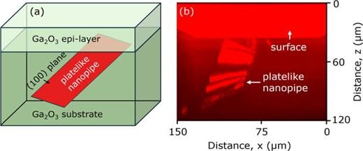
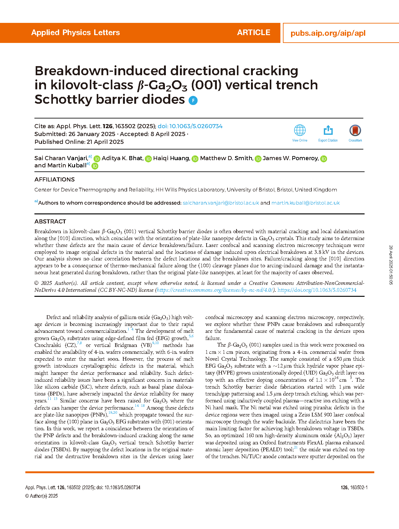
FIG. 1. (a) Schematic showing a plate-like nanopipe defect propagating along the (100) plane in the Ga2O3 substrate. (b) 3D confocal microscope image showing the defect extending through the bulk of the crystal toward the substrate/epi-layer interface.

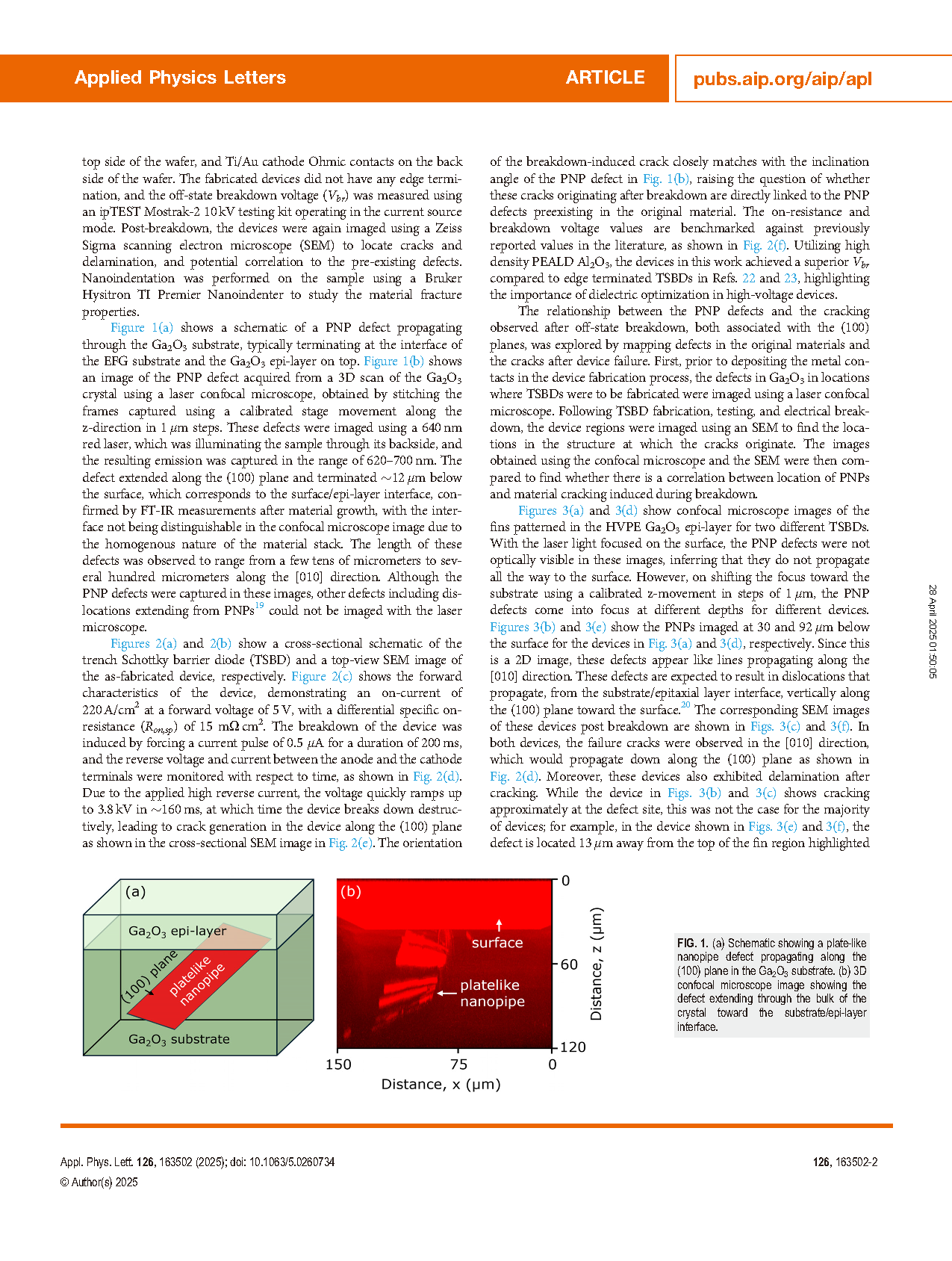
FIG. 2. (a) Schematic of a trench Schottky barrier diode (TSBD). (b) Top view SEM image of an as-fabricated circular TSBD. (c) Forward-IV characteristics and (d) reverse voltage and current characteristics of the TSBD showing a breakdown voltage of 3.8 kV. The reverse voltage and current were monitored as a function of time by forcing a current of 0.5 μA into the device. (e) Post-breakdown cross section SEM image of the TSBD showing a breakdown-induced crack along (100) plane. (f) TSBD performance benchmarked against the literature reports.
DOI:
doi.org/10.1063/5.0260734