


Paper Sharing
【Domestic Papers】The research group led by Academician Sheng Liu from Wuhan University has published a research work entitled “Laser Stealth Dicing of β-Ga₂O₃: Theoretical and Experimental Studies”
日期:2025-05-06阅读:832
The research group led by Academician Sheng Liu, Associate Professor Gai Wu, and Associate Professor Wei Shen from Wuhan University has published an article entitled “Laser Stealth Dicing of β-Ga2O3: Theoretical and Experimental Studies” in the academic journal “Journal of Materials Science & Technology”.
Acknowledgements
This work was funded by the National Natural Science Foundation of China (Grant Nos. 92473102, 62004141, 52202045), the Knowledge Innovation Program of Wuhan-Shuguang (Grant Nos. 2023010201020243, 2023010201020255), the Major Program (JD) of Hubei Province (Grant No. 2023BAA009), the Shenzhen Science and Technology Program (Grant No. JCYJ20240813175906008), the Fundamental Research Funds for the Central Universities (Grant Nos. 2042023kf0112, 2042022kf1028), the Open Fund of Hubei Key Laboratory of Electronic Manufacturing and Packaging Integration (Wuhan University) (Grant Nos. EMPI2024014, EMPI2024021, EMPI2023027), and the China Scholarship Council (Grant No. 202206275005).
Introduction
Ga2O3 is an ultra-wide bandgap (UWBG) semiconductor material with a large bandgap, a high Baliga’s figure of merit, and a high breakdown voltage. Ga2O3 has five polymorphs, with β-Ga2O3 being considered the most promising due to its highest stability and lower cost. β-Ga2O3 is often used in high-power devices due to its excellent performance. High-performance β-Ga2O3-based high-power devices rely heavily on precise processing. However, the anisotropic mechanical properties and cleavage of crystal planes in β-Ga2O3 make it challenging to achieve high-quality wafer dicing using traditional methods during the production of β-Ga2O3-based devices. Currently, there is limited research on wafer dicing of β-Ga2O3. Therefore, it is crucial to explore methods for achieving high-quality wafer dicing of β-Ga2O3. Laser stealth dicing (LSD) is an innovative laser technology that utilizes a focused laser to create subsurface modifications in the wafer without surface damage. Compared with mechanical dicing or laser surface scribing, LSD can effectively prevent damage to the wafer surface and reduce splash contamination during processing. Therefore, LSD is considered a practical method for wafer dicing and has been widely used in wide bandgap semiconductor materials, such as SiC, GaN, and diamond. LSD is typically performed using a diode-pumped solid-state laser, which penetrates the material surface and focuses the laser energy at a predetermined depth. When the laser power density inside the material exceeds the critical threshold, it generates a modified layer characterized by amorphization, dislocations, and microcracks. These internal modifications weaken the material along the laser path, enabling subsequent mechanical separation and fracture. However, excessive energy input can cause unnecessary thermal damage, leading to a decline in crystal performance and an increase in dislocation density. Conversely, insufficient energy input may result in inadequate internal stress for effective cracking. Therefore, the primary challenge is to understand the impact of input energy on the cracking process and the quality of the fracture surface. In recent years, some researchers have explored and reported the mechanisms of the LSD process for SiC, GaN, and diamond via finite element model simulations, MD simulations, and experimental observations. However, there are few reports on the LSD process for β-Ga2O3 and the microscopic mechanisms associated with it.
Abstract
Gallium oxide (Ga2O3) is an ultra-wide bandgap semiconductor with excellent potential for high-power and ultraviolet optoelectronic device applications. High-performance Ga2O3-based high-power devices rely heavily on precise processing, especially in wafer dicing. Laser stealth dicing (LSD) is an innovative laser technology that utilizes a focused laser to create subsurface modifications in the wafer without surface damage. LSD has broad application prospects in the field of semiconductor precision processing. In this work, the idea of achieving high-quality dicing of β-Ga2O3 wafers via LSD was proposed. A combination of atomistic simulations and experiments was used to understand the underlying mechanism of LSD of β-Ga2O3 wafers. On the one hand, the laser loading and fracture process of β-Ga2O3 wafers were simulated using molecular dynamics (MD) methods as well as a machine learning potential. The effects of single-pulse energy on LSD were analyzed through the lattice residual pressure, the final total energy of system, the internal atomic strain, and the maximum stress value during uniaxial tension. On the other hand, based on the MD simulations, LSD was successfully performed on β-Ga2O3 wafers along three main crystal planes in the laboratory, resulting in good surface quality. This work not only provides profound optimization strategies for the LSD process of β-Ga2O3, establishing the foundation for high-quality dicing of β-Ga2O3 wafers, but also verifies the accuracy of MD simulations in predicting trends related to the LSD, offering a potential approach for high-quality dicing of other materials in future research.
Highlights
This work presents the first systematic investigation of the laser stealth dicing process for β-Ga2O3. No prior comprehensive research on this topic has been reported in the literature.
The work innovatively combines molecular dynamics simulations with experimental methods to explore the laser stealth dicing of β-Ga2O3 and its underlying microscopic mechanisms. This integrated research methodology is uncommon in the field of β-Ga2O3
Guided by molecular dynamics simulations, the experimental realization of high-quality laser stealth dicing for β-Ga2O3 wafers was successfully achieved, demonstrating superior fracture surface quality.
Conclusion
In this work, the idea of achieving high-quality dicing of β-Ga2O3 wafers via LSD is proposed. A combination of atomistic simulations and experiments is used to understand the underlying mechanism of LSD in β-Ga2O3 wafers. Firstly, the MD simulation method and a machine learning potential are used to simulate the laser loading and β-Ga2O3 wafer cracking process. By analyzing the lattice residual stress, the final total energy of the system, the internal atomic strain, and the maximum stress value during uniaxial tension, several trends can be observed. As the single-pulse energy of the laser increases, both the residual lattice stress and the final total energy of the system increase. This leads to more significant internal atomic strain. Meanwhile, the maximum stress during the uniaxial tensile process decreases. These factors collectively facilitate wafer cracking of β-Ga2O3. Further observation of the fracture morphology after tensile testing leads to the conclusion that appropriately increasing the laser single-pulse energy not only facilitates the wafer cracking of β-Ga2O3 but also improves the surface quality of the fracture. However, excessive single-pulse energy can be detrimental to the dicing of β-Ga2O3 wafers. LSD of β-Ga2O3 conducted in the laboratory shows that the surface roughness of the three main crystal planes of β-Ga2O3 initially improves and then deteriorates with the increase of single-pulse energy. This is in complete agreement with the theoretical trends observed in the MD simulations. At a suitable single-pulse energy, the (100) surface quality is the best, with an Ra of 0.033 μm, which is superior to the surface quality reported for SiC after LSD. The surface quality of the (010) plane is relatively stable and also exhibits good fracture surface quality.
This work utilizes an innovative research approach to investigate the LSD process of β-Ga2O3 wafers. On the one hand, LSD is successfully performed on β-Ga2O3 wafers in the laboratory under the guidance of MD simulations, resulting in good fracture surface quality. On the other hand, this work demonstrates that MD simulations provide practical guidance for the LSD process of β-Ga2O3 wafers. This work not only provides profound optimization strategies for the LSD process of β-Ga2O3, establishing the foundation for high-quality dicing of β-Ga2O3 wafers, but also verifies the accuracy of MD simulations in predicting trends related to the LSD of β-Ga2O3, offering a potential approach for high-quality dicing of other materials in future research.
Graphics
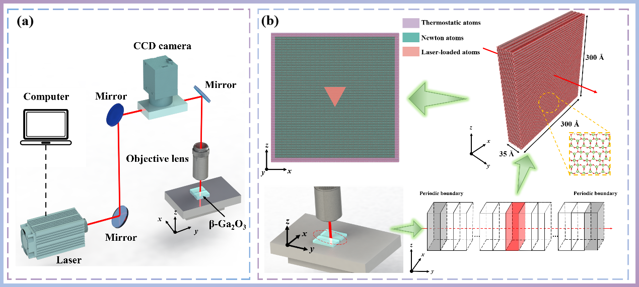
Fig. 1. (a) Schematic diagram of laser processing β-Ga2O3. (b) Three-dimensional MD model of β-Ga2O3.
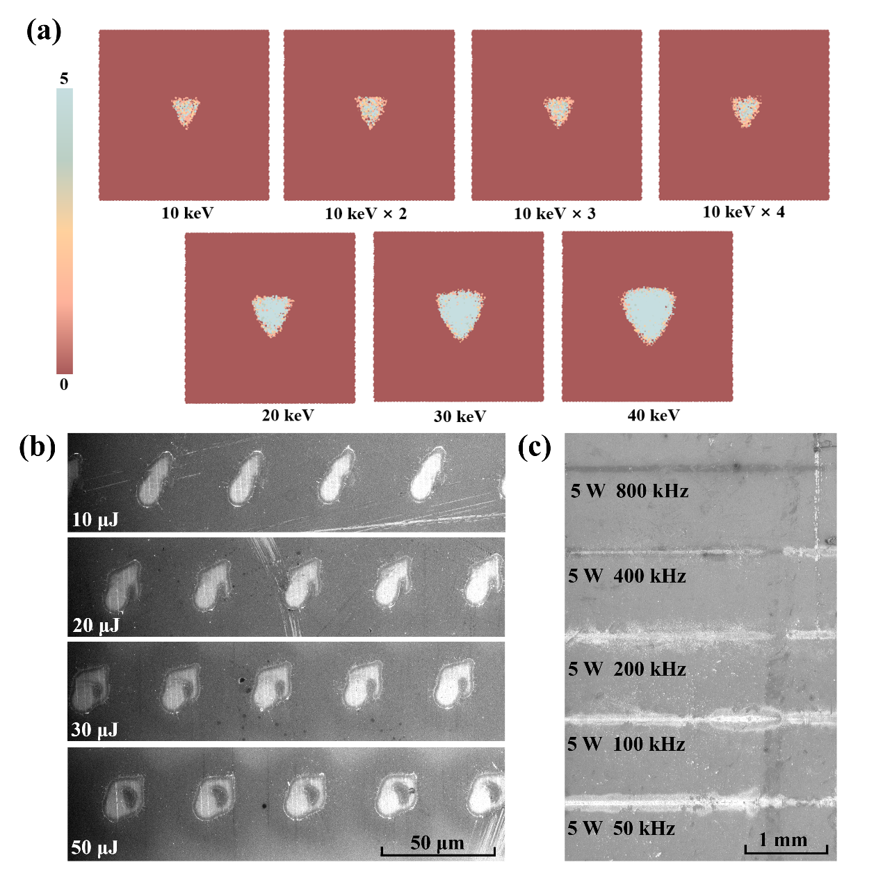
Fig. 2. (a) Internal atomic strain distribution map of β-Ga2O3 after laser loading with different input energies. (b) The morphology of surface damage after laser loading with different single-pulse energies in the experiment. (c) The morphology of surface damage after laser loading with different repetition frequencies in the experiment.
DOI:
doi.org/10.1016/j.jmst.2025.03.044
