


Discover
【Knowledge Discover】Common Process Issues of Gallium Oxide Ultra-High Voltage Optical Switch PCAS and SiC Waveguide AR Glasses - Light Incidence and Surface Reflection
日期:2025-06-05阅读:1459
(This article is reposted from a personal WeChat offical account.)
Many friends left article author comments and gave a good suggestion, saying if you are afraid of leakage between the two gates of your SJ BDS device, could you also etch off an additional part of the p-NiO or p-GaN in the middle area or thin it a little... That makes a lot of sense.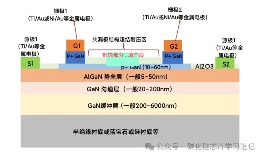
The author can't handle the NiO on his own side and needs to frequently seek help from collaborating teachers. So the progress of this bidirectional SJ BDS device has been very slow recently. Let's continue to study the Gallium Oxide high-voltage photoconductive auxiliary switch.
There are many projects in the US conducting research on Gallium Oxide ultra-high voltage photoconductive switch devices, but there is very little information available. Recently, I have no choice but to draw on the research issues in their Silicon Carbide photoconductive switch devices again.
One of them is the problem of surface reflection of light on Silicon Carbide or Gallium Oxide wafers and internal reflection at the bottom, as well as the surface flashover and burning problem caused by uneven electric field distribution and light distribution.
Adding mirror coating or packaging with a few mirrors around is an option, but it increases cost complexity and shock resistance, and is not conducive to miniaturization and integration.
There are several other options, including how to evenly distribute the electric field over a whole wafer surface and how to reduce surface reflection issues. Sometimes surfaces can reflect more than 30 percent of light, which is a serious problem.
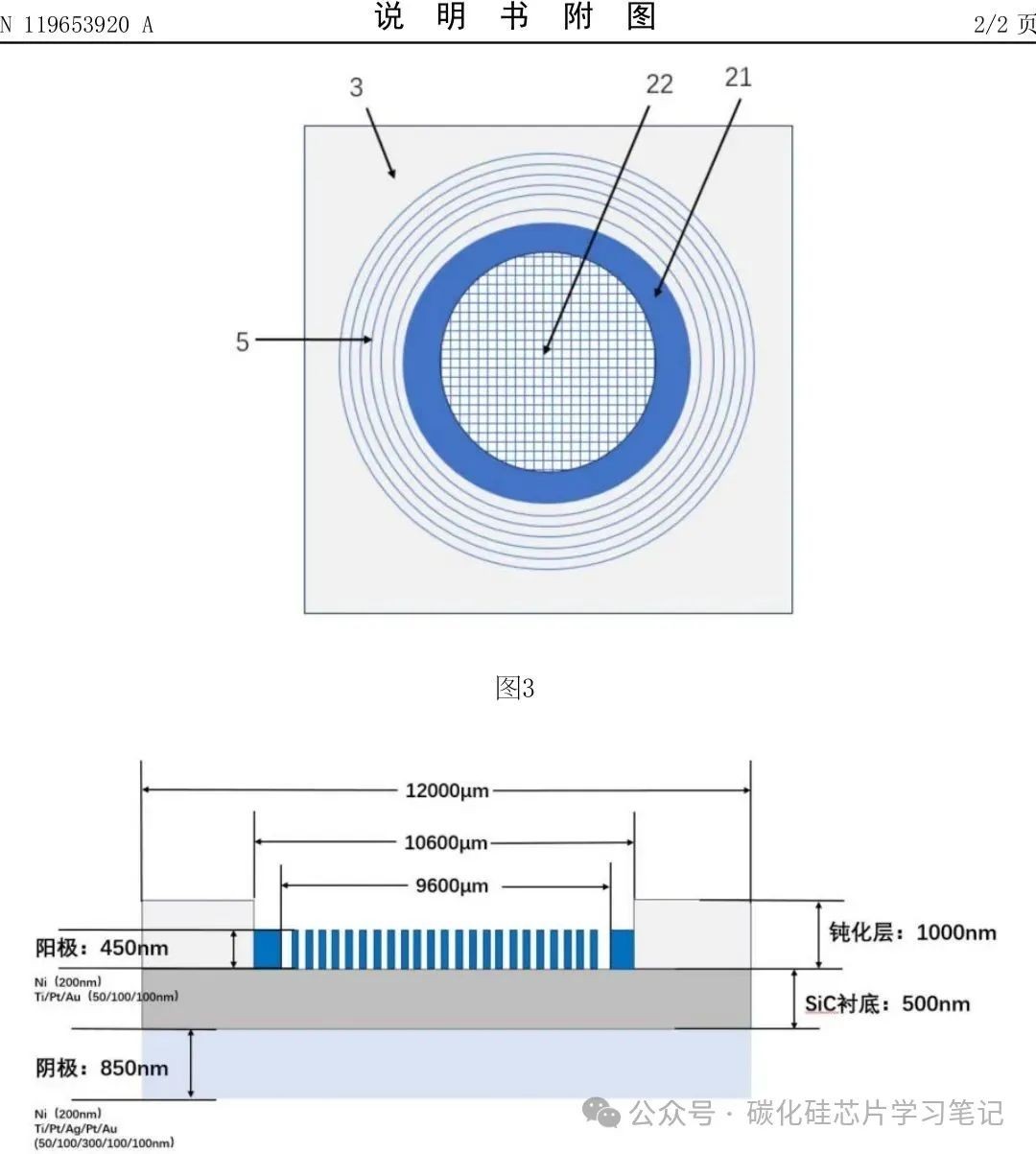
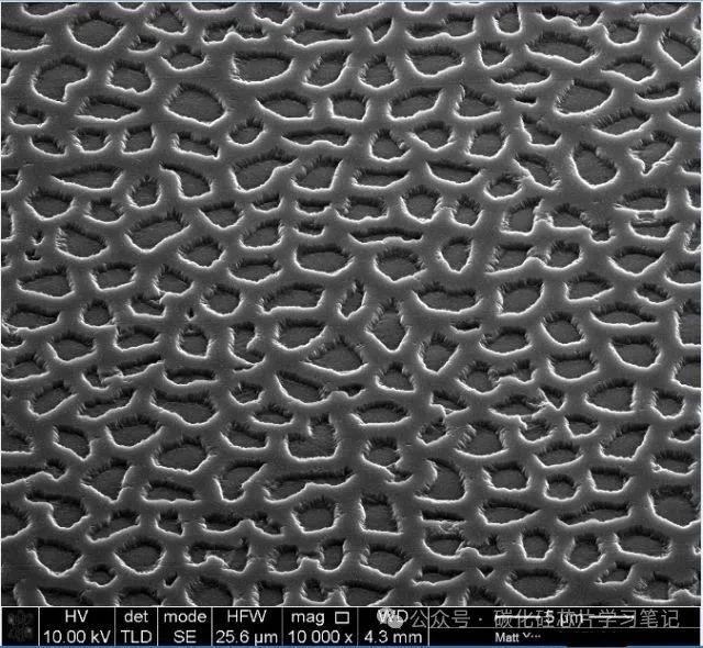
It would be beneficial to significantly reduce surface reflection if sub-micron-hundred-nanometer periodic and hundreds of nanometers deep anti-reflection structures could be etched on the wafer surface comparable to the wavelength.
The problem is that it is really not easy to etch sub-micron anti-reflection structures with a period size and depth of several hundred nanometers on the surface of 4/6/8-inch Silicon Carbide wafers.
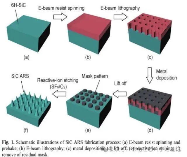
This is a problem related to the Silicon Carbide AR glasses issue. Besides the high cost of Silicon Carbide wafers, the key issue with the current Silicon Carbide AR glasses is how to etched sub-micron and hundred-nanometer periodic micro-nano structures on the surface of this high-hardness and difficult-to-process material.
By the way, the author actually did this before. And nearly a decade ago, a four-inch Silicon Carbide wafer cost tens of thousands of yuan, engraving one was a real headache.
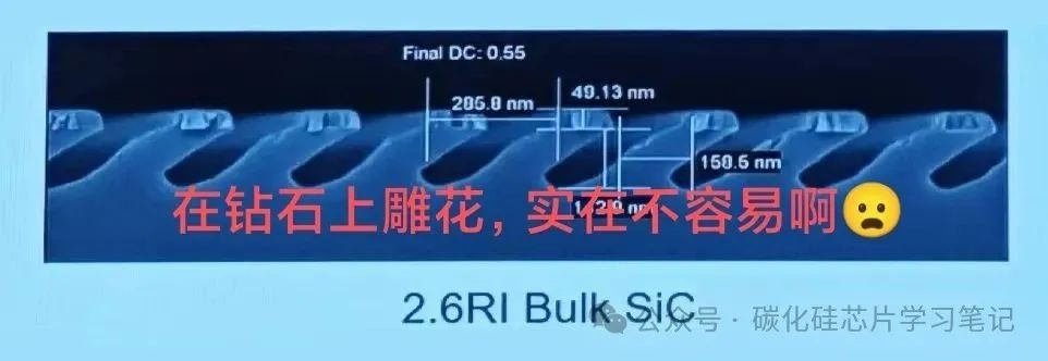
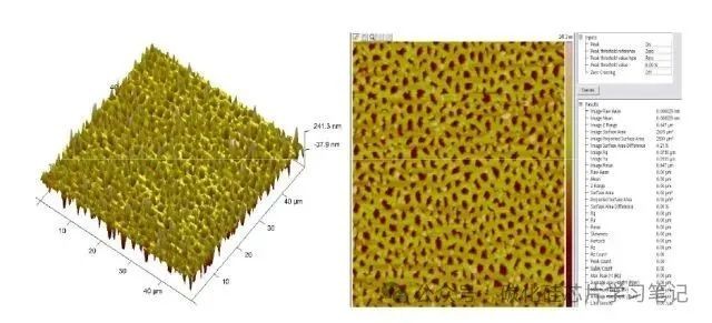
However, once the illuminated part of the entire Silicon Carbide wafer surface is etched into periodic micro-nano structures of several hundred nanometers, it looks really beautiful under the AFM.
At this point, when exposed to light, the surface reflection problem was much better, and the surface reflection was reduced by more than 30 percent.
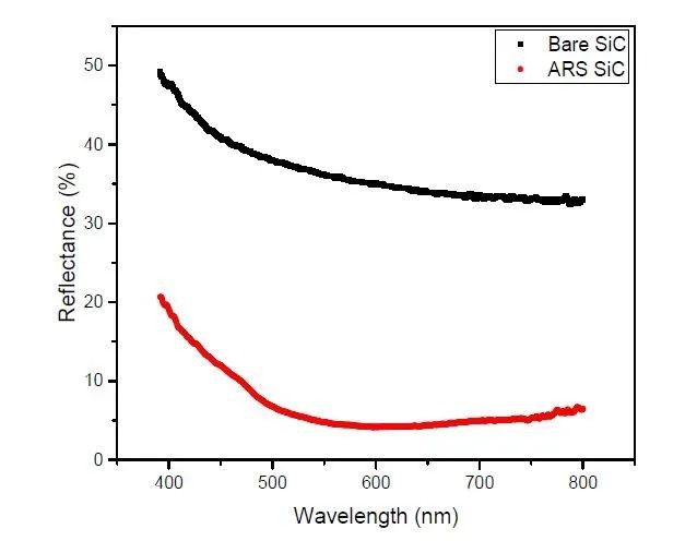
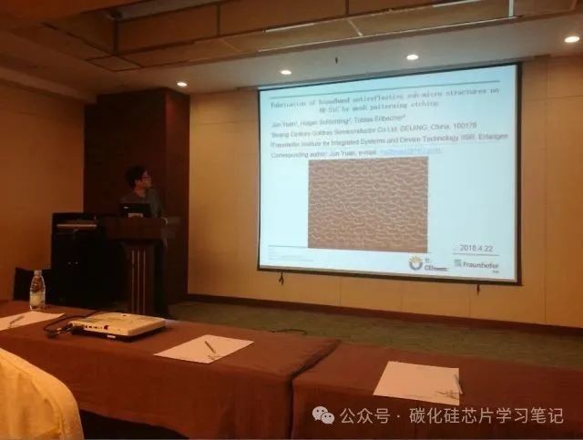
Take a look. The sub-micron anti-reflection structure on the surface of Silicon Carbide etched by the author ten years ago and its light transmission enhancement test data are very beautiful. The key point is that author’s technology doesn't even require a photolithography machine. Not to mention the ASML immersion ArF photolithography machine that the friends in their circle who are now working on Silicon Carbide AR lenses are looking for everywhere. This is a photolithography machine that only exists on the 12-inch advanced process line and the 45nm line...
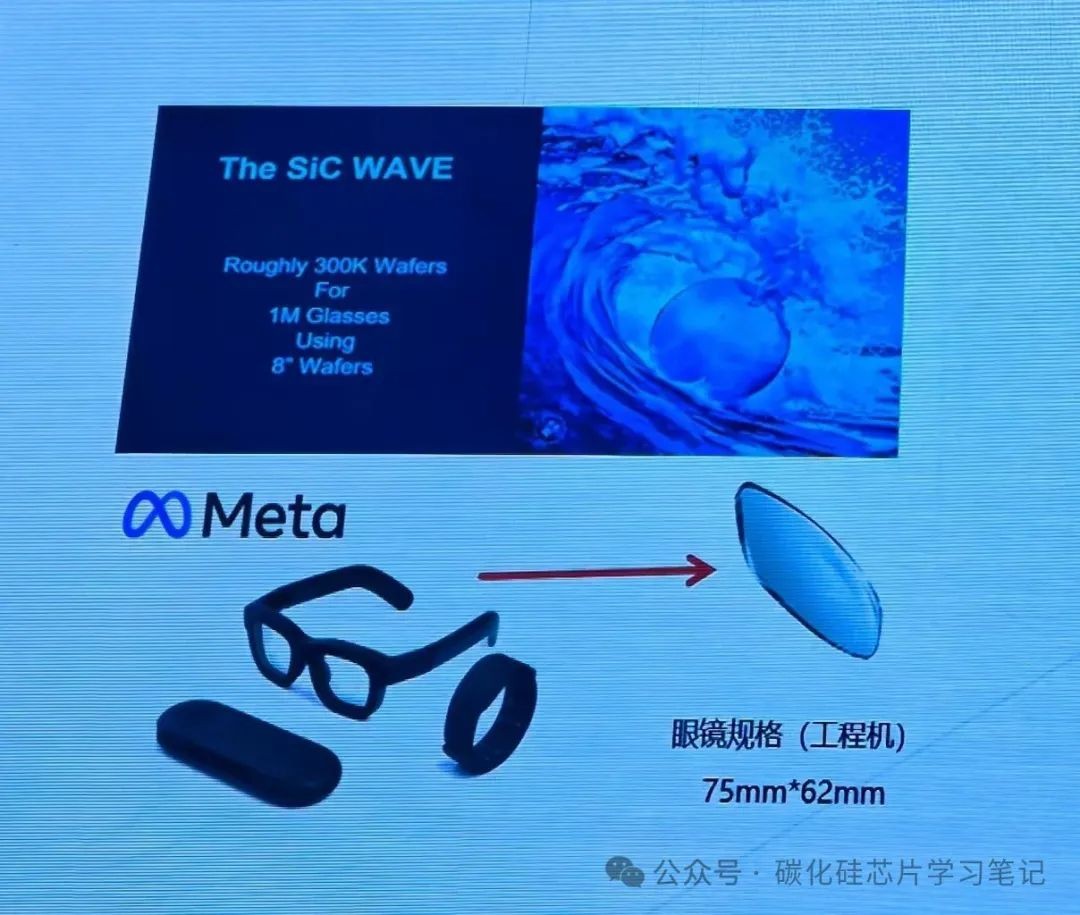
Although major consumer electronics companies, mobile phone manufacturers, and wearable IoT companies are all enthusiastically discussing Silicon Carbide AR glasses technology at present, it is really not easy to find a production line that can do it when it comes to actually implementing it.
