


Discover
【Knowledge Discover】Interpretation of FinFET Technology
日期:2025-06-10阅读:2631
Since the advent of semiconductor transistors, integrated circuit technology has developed rapidly under the guidance of Moore's Law. Moore's Law predicted that the number of transistors per unit area would double every two years, and this progress has been fully validated over the past few decades.
However, as technology nodes move into the nanoscale, traditional planar metal-oxide-semiconductor field-effect transistors (MOSFETs) are facing tough technical challenges. Short channel effects and leakage current problems make planar MOSFETs difficult to meet the demands of deep sub-micron technology nodes. Against this backdrop, fin field-effect transistors (FinFETs) emerged as the successor to planar MOSFETs, offering new possibilities for the continuation of Moore's Law.
This article will review the technological evolution from planar MOSFETs to FinFETs, exploring their core principles and the challenges that lie ahead.
Conventional planar MOSFETs achieve transistor scaling through complementary metal-oxide-semiconductor (CMOS) technology, thereby enhancing the performance and density of integrated circuits. However, when the technology node approaches the sub-100 nanometers level, the reduction in transistor geometry causes a series of problems. First, the short channel effect leads to a decrease in the gate's control over the channel, resulting in a significant increase in leakage current. Secondly, as the gate length (Lg) shortens, the subthreshold slope deteriorates and the switching performance of the transistor is affected.
Figure 1 shows the simulation results of the subthreshold characteristics of a conventional planar MOSFET at different gate lengths, indicating that the shortening of the gate length leads to a deterioration of the subthreshold slope, resulting in a significant increase in leakage current (Ioff).
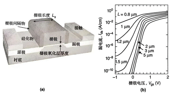
Figure 1 (a) schematic diagram of the traditional planar MOSFET, (b) simulation of increased leakage current as the gate length shortens.
The increase in leakage current directly leads to higher power consumption and increased circuit noise, which poses a serious challenge to the design of mobile devices and high-performance computing systems. In addition, as transistor density increases, the adjustment of doping concentration becomes more complex, further exacerbating the leakage problem. Although the thinning of oxide layers and the introduction of high κ dielectric materials have alleviated these problems to some extent, these improvements have not fundamentally addressed the challenges of short-channel effects and leakage currents.
In response to the limitations of planar MOSFETs, the semiconductor field began to explore new transistor structures.
FinFET, as a three-dimensional transistor structure, achieves three-dimensional control of the channel by forming multiple vertical fin-like structures (Fins) on a silicon substrate. This structure enables the gate to encircle the channel more effectively, thereby enhancing the gate's control ability and reducing leakage current.
The concept of FinFET was originally proposed by a research team at the University of California, Berkeley (including Chenming Hu, Tsu-Jae King-Liu and Jeffrey Bokor, etc.) on SOI (insulator silicon) substrates. SOI substrates provide a good foundation for the performance optimization of FinFET by reducing parasitic capacitance and leakage current.
Subsequently, companies such as Samsung further extended FinFET technology to bulk silicon substrates, suppressing leakage current by heavy doping beneath the fins. Although this approach affected FinFET performance to some extent, it laid the foundation for mass production.
The core advantage of FinFET lies in its three-dimensional structure. Compared with traditional planar MOSFETs, FINFETs exhibit lower leakage current and higher switching ratio at the same technical node. This enables FinFET to maintain excellent electrical properties at deep nanotech nodes such as 5 nanometers, 3 nanometers and even smaller, thus extending the life of Moore's Law.
Despite the significant technological advancements in FinFET, there are still many challenges in its large-scale manufacturing and performance optimization. First, the three-dimensional structure of FinFET demands higher precision in the manufacturing process, which increases manufacturing costs and technical difficulty. Secondly, as the technology node shrinks further, the fin width and height of the FinFET need to be more refined, which puts higher demands on the process capabilities of the equipment.
In addition, the electrical performance of the FinFET still needs to be further optimized. Although FinFETs perform well in suppressing leakage current, their current-carrying capacity (such as carrier mobility) may be affected by fin structure and contact resistance. Therefore, finding the balance point between FinFET's structural design and material selection is a key issue for the future.
FinFET Structures and Their Advantages in Microelectronic Devices
FinFET, with its unique three-dimensional structure and significant performance advantages, plays a crucial role in the design and manufacture of microelectronic devices.
The basic structure of FinFET is shown in Figure 2, including a fin transistor constructed on an SOI (silicon insulated substrate) or bulk silicon substrate and its longitudinal profile. The core feature of a FinFET is that its conductive channels are wrapped by thin silicon fins, which form the main body of the device. The fin thickness measured from the source to the drain direction directly determines the effective channel length of the device. The body region of the FinFET is designed to be ultra-thin compared to traditional planar MOSFETs, and the electrical control of the channel is greatly enhanced by controlling the electric field on three sides (instead of the traditional single-sided top control).
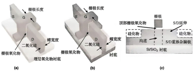
Figure 2 FinFET structure: (a)SOI substrate; (b) bulk substrate; (c) longitudinal cross-sectional view
The optimization of this structure enables FinFET to perform well in terms of size scaling. When the fin thickness is equal to or less than the gate length (Lg), the FinFET can effectively suppress the Off-state leakage current, thereby achieving better performance. In addition, since thin fins can be formed using the same process as gate patterns and etching tools, the manufacturing process of FinFETs is relatively simple. More importantly, the ultrathin body region design makes proper doping an option, as silicon regions a few nanometers away from the gate no longer exist, further reducing the complexity of the device.
FinFET's Performance and Design
FinFET's multi-gate configuration is another notable feature of it. In this configuration, the channel is surrounded by gates on multiple surfaces, resulting in better electrical control of the channel. This design not only suppresses the leakage current in the "off state" more effectively, but also significantly boosts the drive current in the "on state", enhancing the device's switching performance. In addition, the multi-gate FinFET shows better intrinsic gain and lower channel length modulation capability in analog circuits, which gives it a unique advantage in high-performance analog applications.
The advantages of FinFET are reflected in several aspects: higher speed, lower leakage, lower supply voltage (Vdd), lower power consumption, better subthreshold swing, no random doping fluctuation, smaller variability, better mobility, and future subthreshold design capabilities. These characteristics make FinFET have broad application prospects in high-performance computing, low-power devices and advanced microelectronic devices.
Figure 3 shows the design parameters of the FinFET's thin body fin and its multi-gate configuration. When designing a FinFET, several key parameters need to be taken into account: fin width, fin height, and fin spacing.
Fin width: The size of the fin width directly affects the Drain Induced Barrier Lowering (DIBL) effect. A smaller fin width can effectively reduce DIBL, thereby improving the switching performance of the device.
Fin height: The choice of fin height is limited by etching technology and requires a trade-off between layout efficiency and design flexibility. Higher fins may affect the scaling ability of the device, while lower fins may limit electrical performance.
Fin spacing: Fin spacing determines the layout area and also affects the source/drain (S/D) injection Angle. A smaller fin spacing can improve layout efficiency, but it may sacrifice device performance.
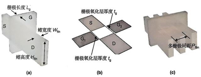
Figure 3 (a) Fin parameters of the double-gate-FinFET: (a) schematic diagram; (b) planar view; (c) Multi-gate configuration
In the manufacturing process of FinFET, the gate-first process and the source/drain (S/D) first process are two main technical routes. The gate-first process, which forms the gate first and uses it as a mask to inject into the source and drain, has the advantage of better self-alignment between the source and drain and the gate. However, in sub-100-nanometer nodes and smaller MOSFETs, high κ dielectric and metal gate stacks must be used due to the physical scaling limit of oxides. In this case, the gate-first process faces challenges in the subsequent injection annealing step, as it is necessary to eliminate injection damage and obtain the desired doping distribution while maintaining stack integrity. To address this issue, the S/D priority process emerged.
At the core of the S/D priority process is the use of sacrificial false gates as injection masks, which are then removed after the annealing step and a new gate stack is constructed. This process effectively addresses the process challenges of high κ dielectric and metal gate stacks.
As shown in Figure 4, the S/ D-first process for forming FinFET on SOI (silicon shell) substrate mainly includes the following steps:
First, pattern through the oxide mask layer and etch to the SOI; Then deposit, pattern and etch on the patterned oxide layer to form a false gate and remove the exposed hard mask oxide, followed by S/D formation and siliconization; Next, deposit insulators to fill the contact grooves and flatten them; Subsequently, the false gate is removed to expose the patterned hard mask through which the fin pattern is transferred by anisotropic etching to the underlying silicon layer; Afterwards, an inner isolation layer is formed on the S/D side wall to ensure sufficient separation between the gate and the extended source and drain; Finally, deposit in the gate groove to form the gate stack.
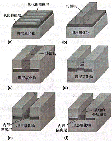
Figure 4 Schematic diagram of the formation of the SOI substrate FinFET: The fabrication method of the source and drain first and then the main fin
The semiconductor industry has achieved remarkable accomplishments in the research and development as well as mass production of FinFETs. Foundries have achieved mass production of 16-nanometer / 14-nanometer FinFETs, and development of 10-nanometer FinFETs is also underway. However, the scalability of traditional FinFETs is gradually being limited as technology nodes continue to shrink.
According to IMEC's technology roadmap, the 7-nanometer node offers two transistor options: FinFET and transverse ring-gate nanowire FET (transverse nanowire FET). For the 5-nanometer node, a transverse nanowire FET is preferred. The transverse nanowire FET is essentially an evolution of FinFETs from double-gate and triple-gate to full-ring gate structures, which further enhance the gate's control over carriers by increasing the gate area, thus enabling more efficient turn-off of the device.

Interuniversity Microelectronics Centre (IMEC) has released a blueprint for processes below 1 nanometer, sharing research and development plans for the corresponding transistor architecture
Although the transverse nanowire FET may be superior to the FinFET in electrostatic properties, its manufacturing process is more complex, especially with greater challenges in the process handling at the bottom of the device. Finfets still face some key challenges in practical applications, including threshold voltage regulation, edge capacitance between the gate and the top/bottom of the source and discharge, parasitic resistance, and device variability. These issues have, to some extent, limited the performance optimization of FinFET in smaller technology nodes.
To sum up, FinFET has become the core technology of sub-100-nanometer semiconductor devices thanks to its unique three-dimensional structure and excellent performance. Despite the complexity of its manufacturing process and some technical challenges, FinFET's successful mass production at the 16-nanometer / 14-nanometer node has demonstrated the maturity of its technology with the continuous optimization of the S/ D-first process and the application of high κ dielectric and metal gate stacks. However, as the technology node shrinks further, it may be necessary to shift to more forward-looking structures, such as the transverse nanofilm FET, to meet future performance requirements.
References:
Semiconductor Manufacturing Handbook
