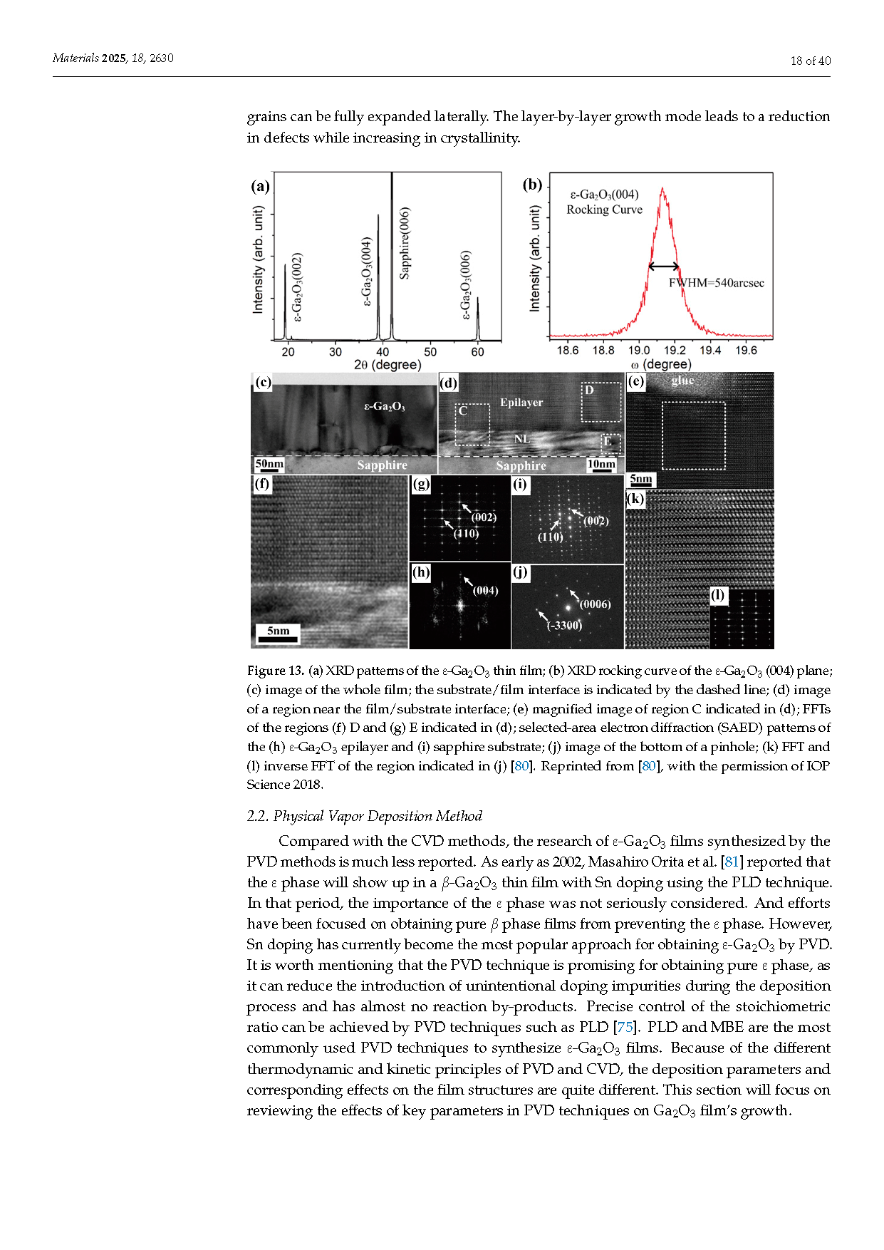
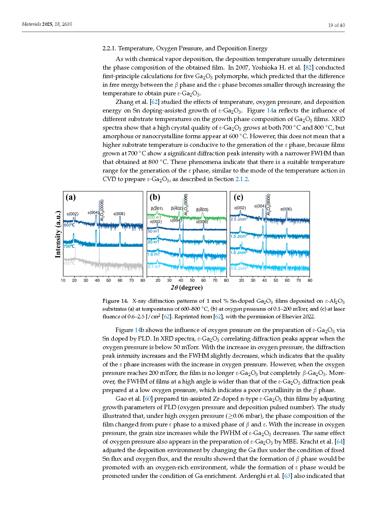
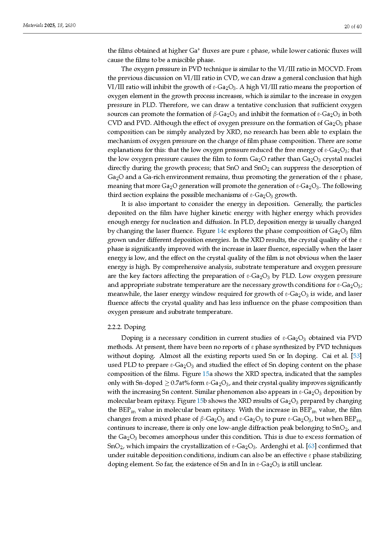
Paper Sharing
【Domestic Papers】Harbin Institute of Technology (Shenzhen) --- A Review of ε-Ga₂O₃ Films: Fabrications and Photoelectric Properties
日期:2025-06-18阅读:701
Researchers from the Harbin Institute of Technology (Shenzhen) have published a dissertation titled "A Review of ε-Ga2O3 Films: Fabrications and Photoelectric Properties" in Materials.
Project support
This work is financially supported by the National Natural Science Foundation of China (grant Nos.52102094), the Guangdong Basic and Applied Basic Research Foundation (grant Nos.2024A1515011678), and the Shenzhen Science and Technology Innovation Committee (grant Nos.JCYJ20220531095017039, KJZD20240903095400001).
Abstract
Gallium oxide (Ga2O3), as an ultra-wide bandgap semiconducting material, has attracted extensive research interest in recent years. Owing to its outstanding electrical and optical properties, as well as its high reliability, Ga2O3 shows great potential in power electronics, optoelectronics, memory devices, and so on. Among all the different polymorphs, ε-Ga2O3 is the second most thermally stable phase. It has a hexagonal crystal structure, which contributes to its isotropic physical properties and its suitable growth on low-cost commercial substrates, such as Al2O3, Si (111). However, there are far fewer research works on ε-Ga2O3 in comparison with the most thermally stable β phase. Aiming to provide a comprehensive view on the current works of ε-Ga2O3 and support future research, this review conducts detailed summarizations for the fabrication processes of ε-Ga2O3 thin films and the photoelectrical properties of ε-Ga2O3-based photodetectors. The effects of different deposition parameters on film phases and qualities are discussed. The forming mechanisms of ε phase prepared by chemical vapor depositions (CVDs) and physical vapor depositions (PVDs) are analyzed, respectively. Conclusions are made concerning the relationships between film microstructures and properties. In addition, strategies for further improving ε-Ga2O3 film performance are briefly summarized.
Summary
In summary, ε-Ga2O3 films can be fabricated via either CVD or PVD techniques. In the case of CVD, substrates play an important role as a base for ε phase formation. Suitable temperatures, pressures, and precursor ratios are required for ε-phase nucleation and pure phase growth. In the case of PVD, doping is a necessary condition for the formation of the ε phase. The quality of film is further affected by substrate type, deposition temperatures, and oxygen pressures. The reported photoelectrical properties of ε-Ga2O3-based photodetectors vary a lot. In general, defects, including grain boundaries, doping-induced lattice distortions, and oxygen vacancies, can generate trapping energy levels and obstacles for the migrations of carriers, leading to low responsivity and slow response of the ε-Ga2O3 films. The optimization of electrode structures and the introduction of passivation layers can strongly enhance the responsivity and detectivity of ε-Ga2O3 films. Special electrode materials can generate build-in electric field in ε-Ga2O3 films to achieve ultrafast responses. Despite the findings of current research, the formation mechanisms of ε-Ga2O3 films remain unclear. Especially, ε-Ga2O3 films without doping have never been successfully synthesized via PVD techniques. The simultaneous improvements of the photoelectrical properties (responsivity, PDCR, detectivity, responding time, etc.) of ε-Ga2O3 are still very difficult to attain. Moreover, many other properties and potential applications of ε-Ga2O3, such as power performance for electronic devices and high electron mobility properties for RF devices, are rarely investigated. It can be expected that, with further understanding of the fundamentals of ε-Ga2O3, the films’ properties can be enhanced significantly and specifically tuned to meet the requirements of a great range of applications.
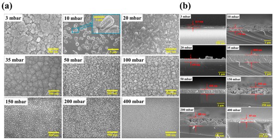
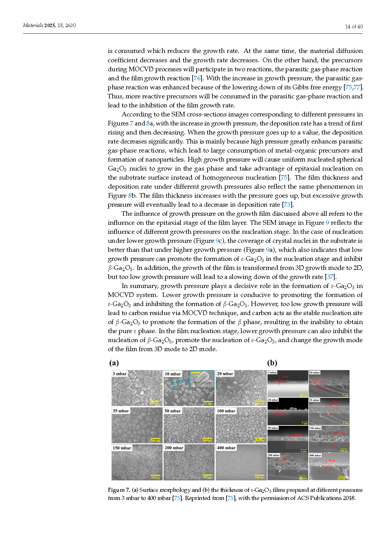
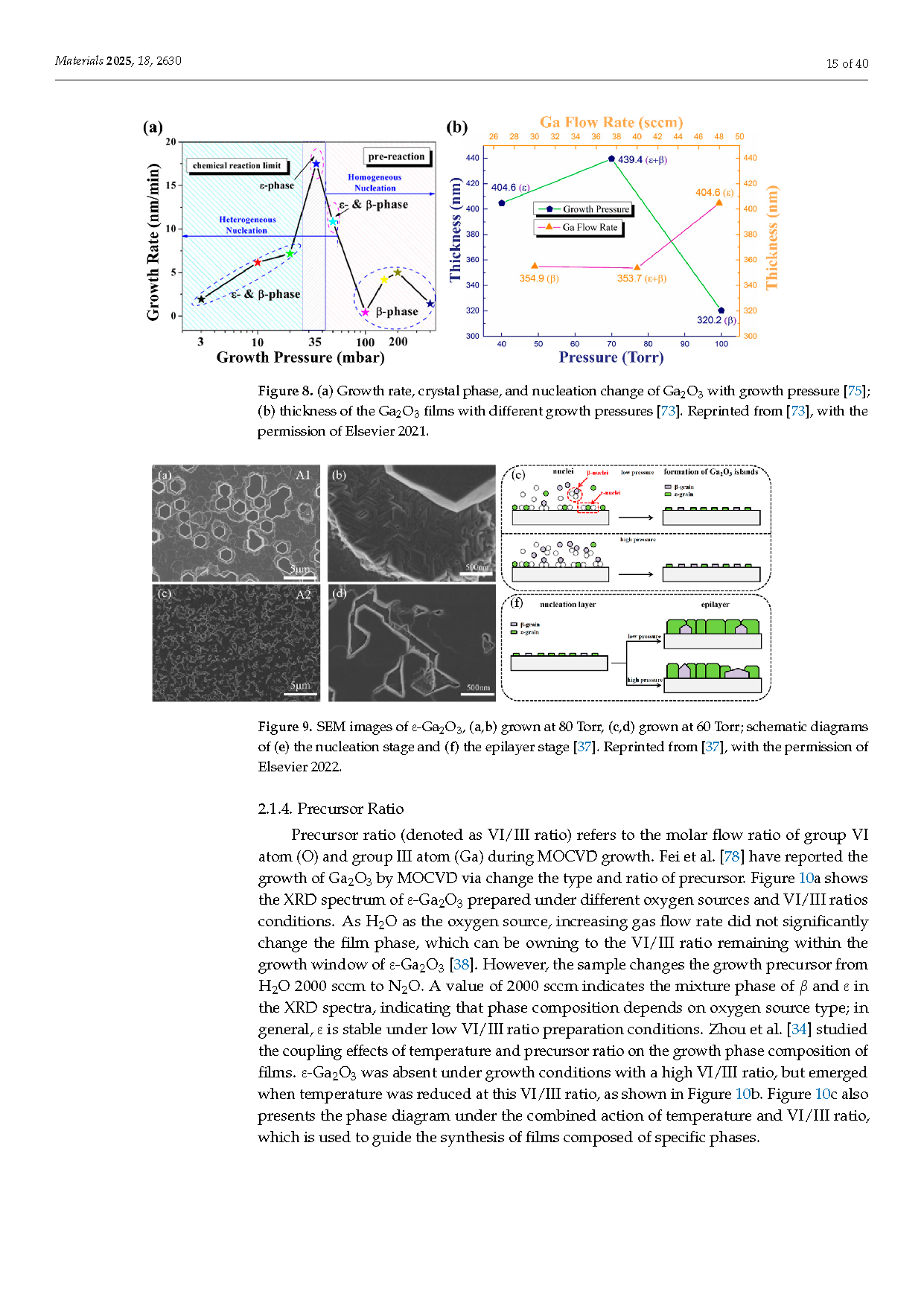
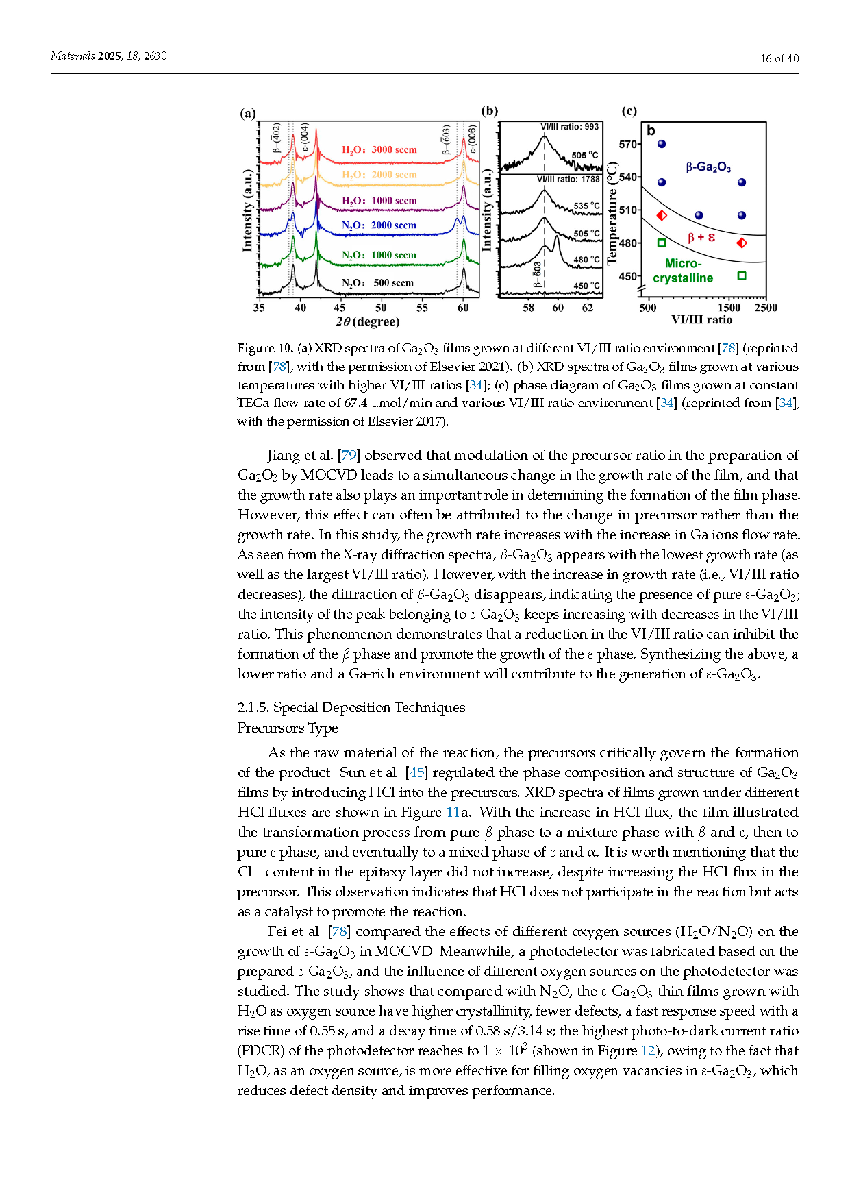
Figure 1. (a) Surface morphology and (b) the thickness of ε-Ga2O3 films prepared at different pressures from 3 mbar to 400 mbar.
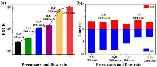
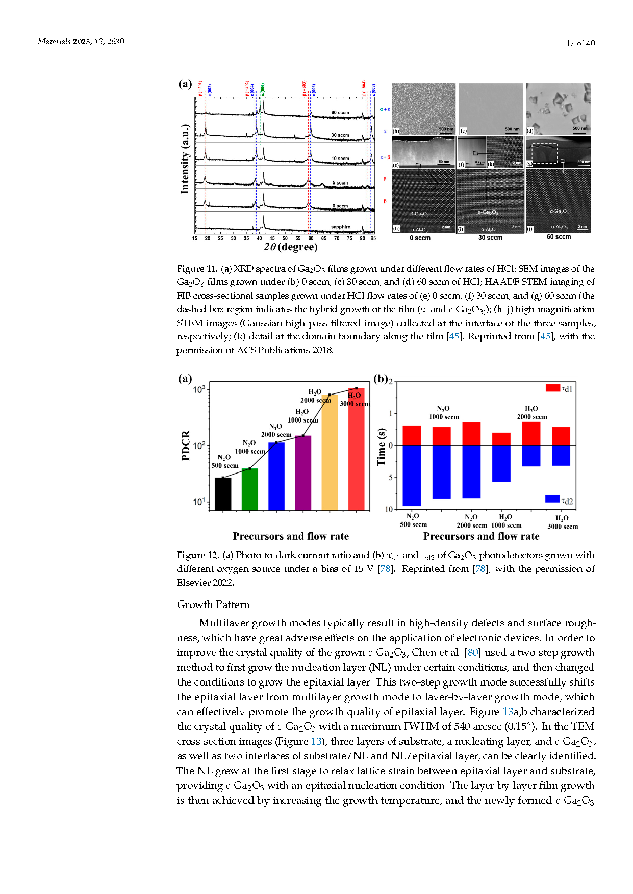
Figure 2. (a) Photo-to-dark current ratio and (b) τd1 and τd2 of Ga2O3 photodetectors grown with different oxygen source under a bias of 15 V.
DOI:
doi.org/10.3390/ma18112630