Paper Sharing
【Domestic Papers】Sun Yat-Sen University --- High performance solar-blind photodetectors based on MOCVD grown β-Ga₂O₃ with hydrogen plasma treatment
日期:2025-06-20阅读:613
Researchers from the Sun Yat-Sen University have published a dissertation titled "High performance solar-blind photodetectors based on MOCVD grown β-Ga2O3 with hydrogen plasma treatment" in Semiconductor Science and Technology.
Project support
This work was supported by the Science and Technology Development Plan Project of Jilin Province, China (No. YDZJ202303CGZH022), Shenzhen Science and Technology Program (GJHZ202209131 42807014, No. 20231127114207001), National Key Research and Development Program (2024YFE0205300), the Open Fund of the State Key Laboratory of Optoelectronic Materials and Technologies (OEMT-2023-KF-05), respectively.
Background
Solar-blind ultraviolet photodetectors (SBPDs) are widely applied in missile tracking, flame detection, non-line-of-sight communication, et al. Many wide bandgap semiconductors can be used to fabricate SBPDs, such as AlGaN, ZnMgO, diamond, and β-Ga2O3. Among these candidates, β-Ga2O3 is a natural solar-blind ultraviolet detection material with a bandgap of 4.9–5.2 eV, showing advantages of high critical breakdown field and excellent radiation resistance [8–10]. The metal–semiconductor–metal (MSM) type β-Ga2O3 SBPDs have gained widespread favor due to their simple manufacturing process and high sensitivity, but their response speed is slow due to the persistent photoconductivity (PPC). Usually, PPC is caused by defects in semiconductor material. In addition, Schottky barrier in MSM structure SBPD will be decreased under light illumination. When the light source is turned off, the recovery of the barrier will take time, also leading to the PPC phenomenon. Simultaneously achieving high responsivity and fast response time has always been the pursuit. Generally, there are two types of contact between metal and semiconductor in the MSM structure SBPDs: Schottky contact and ohmic contact. Considering the Fermi level pinning effect, Schottky contact can be usually formed between the metal and the high-resistance β-Ga2O3 and helps to lower the dark current.
Abstract
The growing demand for efficient solar-blind ultraviolet photodetectors (SBPDs) has fueled interest in the exceptional properties of β-Ga2O3. Here, SBPDs with a metal–semiconductor–metal structure are fabricated based on β-Ga2O3 thin films. The (-201) oriented β-Ga2O3 is grown on c-plane sapphire using metal–organic chemical vapor deposition. Hydrogen as a shallow donor is introduced into the β-Ga2O3 surface layer selectively on the area underneath contacts by plasma treatment to enhance the ohmic contact. As a result, superexcellent performances are demonstrated, including a remarkable responsivity of 3.0×10⁴ A W−1 at a wavelength of 238 nm, specific detectivity of 1.2×10¹⁷ Jones and an external quantum efficiency of 1.5×10⁷%. Also, faster rise and decay speed are achieved. The hydrogen plasma treatment (HPT) brings fast transit time of carriers and effective gain electron injection, which are used to explain the enhancement of performance. This work highlights that HPT selectively on the area underneath contacts is an efficient strategy for achieving high-performance β-Ga2O3 solar-blind ultraviolet photodetectors.
Conclusion
In conclusion, high-performance SBPDs based on β-Ga2O3 thin film with a MSM structure were successfully fabricated. By employing a selective HPT on the areas beneath the contacts, shallow donor states were introduced, significantly improving the ohmic contact properties. This modification facilitated faster carrier transit times and effective gain electron injection, resulting in exceptional device performance. The fabricated photodetectors achieved a remarkable responsivity of 3.0 × 10⁴ A W−1, a specific detectivity of 1.2 × 10¹⁷ Jones, an EQE of 1.5 × 10⁷% and faster response speed. These results highlight the efficacy of selective HPT in enhancing the optoelectronic properties of β-Ga2O3-based photodetectors, offering a promising pathway for advancing high-performance solar-blind ultraviolet photodetection technologies.
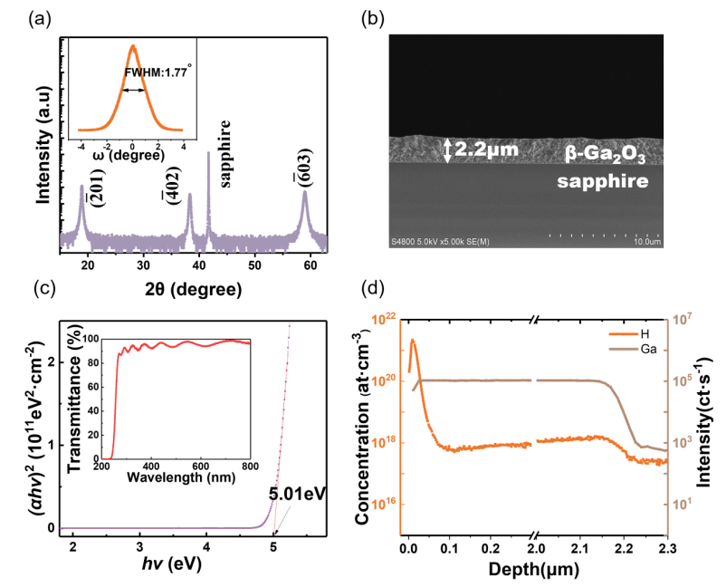
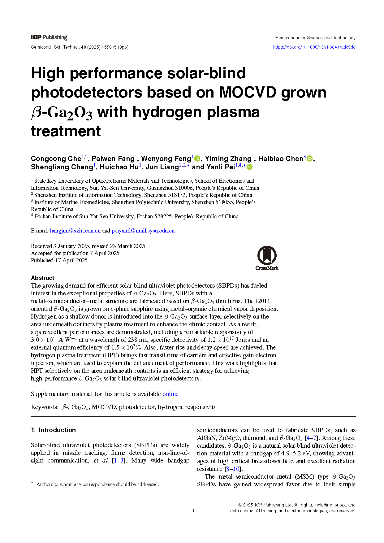
Figure 1. (a) XRD patterns of the β-Ga2O3 thin film grown on c-plane sapphire substrates, and inset is the XRD rocking curve of the β-Ga2O3 (-201) diffraction peak. (b) SEM image of the cross-sectional morphology. (c) Optical bandgap of β-Ga2O3 thin film. The inset shows the optical transmittance spectrum. (d) SIMS depth profiles of the H plasma treated β-Ga2O3 film.
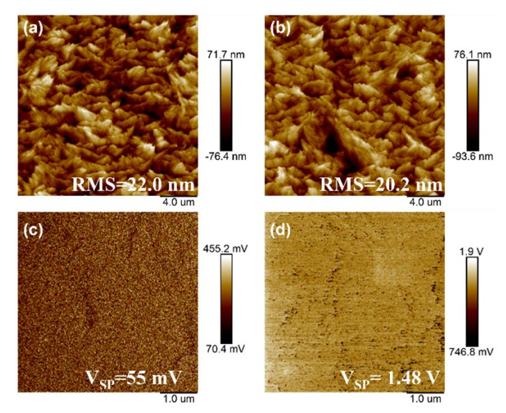
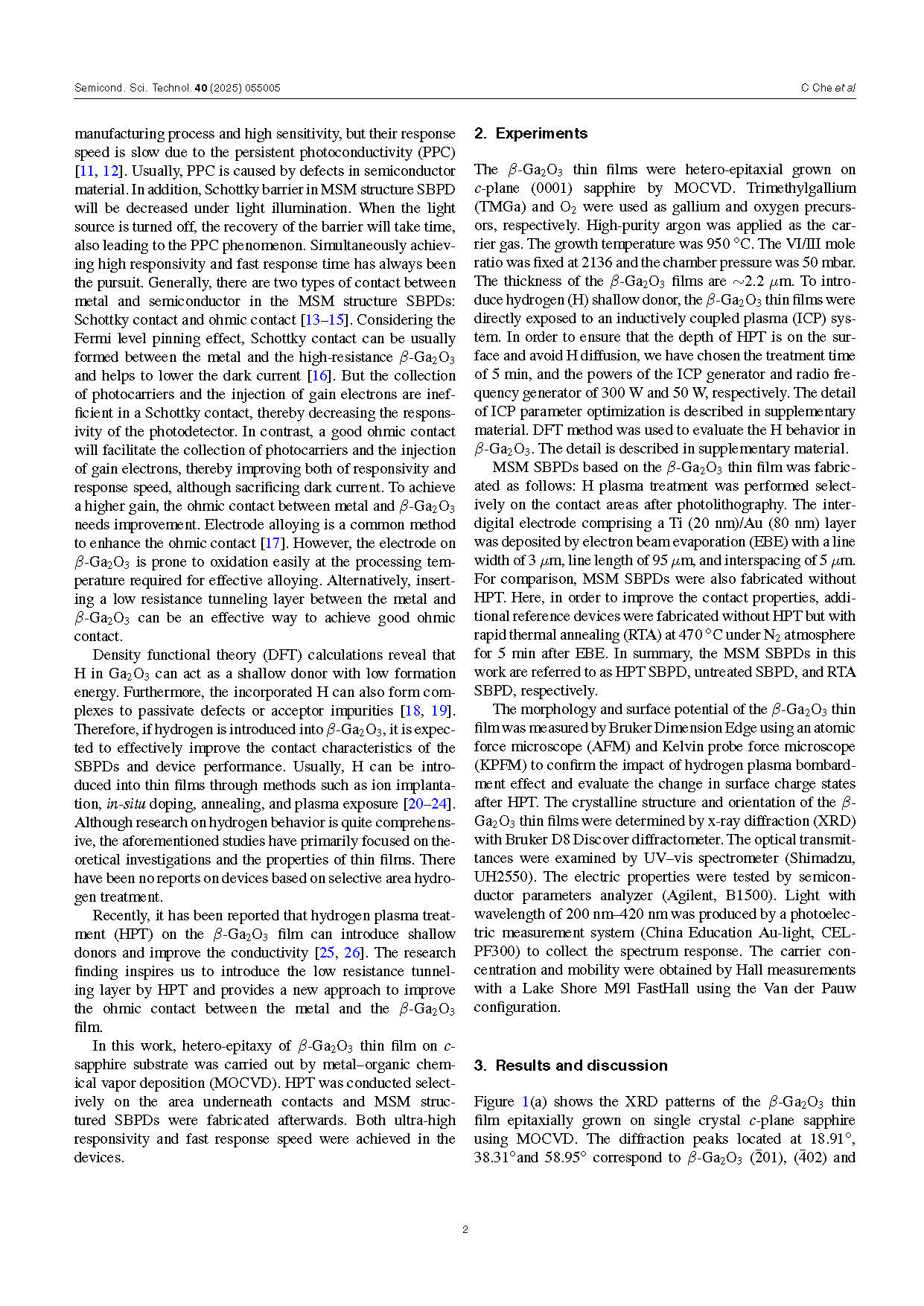
Figure 2. AFM morphologies of β-Ga2O3 with different surface treatment. (a) Without H plasma treatment. (b) With H plasma treatment. KPFM morphologies of β-Ga2O3 with different surface treatment. (c) Without H plasma treatment. (d) With H plasma treatment.
DOI:
doi.org/10.1088/1361-6641/adc9dd