


Member Intro
【Member Intro】Xiamen University——Council Member
日期:2023-03-06阅读:1181
Introduction
Founded in 1923, the Department of Chemistry of Xiamen University is one of the first science departments to be established in the initial stage. Since the establishment of the College of Chemistry and Chemical Engineering, the College has adhered to the motto of "Pursue excellence, strive for perfection", accumulated strong capabilities to carry out scientific researches, and has built five national scientific research platforms, including the "National Key Laboratory of Solid Surface Physics and Chemistry".
Figure: Logo of College of Chemistry & Chemical Engineering, Xiamen University; Logo of Tan Kan Kee Innovation Laboratory
Established in 2019 with the approval of the Fujian Provincial Government and supported by Xiamen University, the Tan Kan Kee Innovation Laboratory is one of the first four provincial innovation laboratories in Fujian. It is committed to tackling “bottleneck” problems and promoting the industrialization of high-tech achievements. Through the innovation system and mechanism, it gathers domestic and foreign innovation resources to build a "technology accelerator" and "industrial engine" in the field of energy and semiconductor materials, and contribute to building China into a science and technology power of the world.
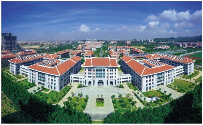
Figure: Tan Kan Kee Innovation Laboratory platform of Xiamen University
The scientific research platform has large analytical equipment such as X-ray diffractometer (XRD), spherical aberration electron microscope, 300KV high resolution transmission electron microscope (HRTEM), X-ray photoelectron spectroscopy (XPS), steady-state transient photoluminescence spectrometer (PL), electron paramagnetic resonance spectrometer (EPR), which can provide complete test characterization for the implementation of gallium oxide project. In addition, the Tan Kan Kee Innovation Laboratory has a variety of advanced micro nano processing and testing equipment, such as the quietest noise-free laboratory in Asia, molecular beam epitaxy system, electron beam exposure system, ultra-low temperature semiconductor testing system, etc., which will provide strong support for the development of this project.

Figure:Micro nano processing platform in Tan Kan Kee Innovation Laboratory
Introduction to relevant businesses
Gallium oxide (Ga2O3) is a new wide band-gap semiconductor since silicon carbide (SiC) and gallium nitride (GaN). It has the advantages of good thermal stability, wide band gap, large ultraviolet absorption coefficient,and it is easy to process. It has been widely applied in deep ultraviolet photoelectric detection and ultra-high voltage power devices. The photoelectric detector made of gallium oxide can achieve high sensitivity, low false alarm rate and good anti-interference, and enhance the situation recognition ability in many key application scenarios such as missile tracking, fire early warning and deep space detection. In terms of power components, it can achieve higher resistance to high voltage, smaller volume, lower loss, and effectively reduce energy consumption in new energy vehicles, rail transit, renewable energy power generation and other fields. By 2030, the market of Ga2O3 semiconductor is predicted to reach 1.5 billion US dollars. Our R&D team focuses on the development of high-quality epitaxial Ga2O3 thin film growth and preparation technology as well as the systematic regulation of photoelectric performance. Focusing on the key scientific issues such as Ga2O3 micro electronic structure, defects and doping mechanism, we have carried out researches on high-quality epitaxial Ga2O3 thin film growth, development of photodetector , development of high-power high-speed electronic device and other new semiconductor devices. At this stage, we have accumulated some achievements.

Figure:Ga2O3 photodetector and its package, Ga2O3 film epitaxy
Introduction of R&D Team
Relying on the School of Chemistry and Chemical Engineering of Xiamen University, the R&D team focuses on cutting-edge interdisciplinary researches such as semiconductor physical chemistry, semiconductor device physics, and surface physical chemistry, and is committed to developing new photoelectronic materials and devices. At present, the focus of the research and development is the preparation of metal oxide semiconductor thin films, the regulation of surface and photoelectric properties, and the development of Ga2O3 based photoelectronic devices. The team has established long-term cooperation with domestic and foreign synchronized radiation light sources and multiple research groups. Currently, there are 18 main members, and so far, the team has published more than 140 papers in Nat Commun.、J. Am. Chem. Soc.、Phys. Rev. Lett.、Adv. Mater. and other journals .
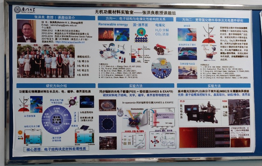
Figure: Achievements display of the R&D Team
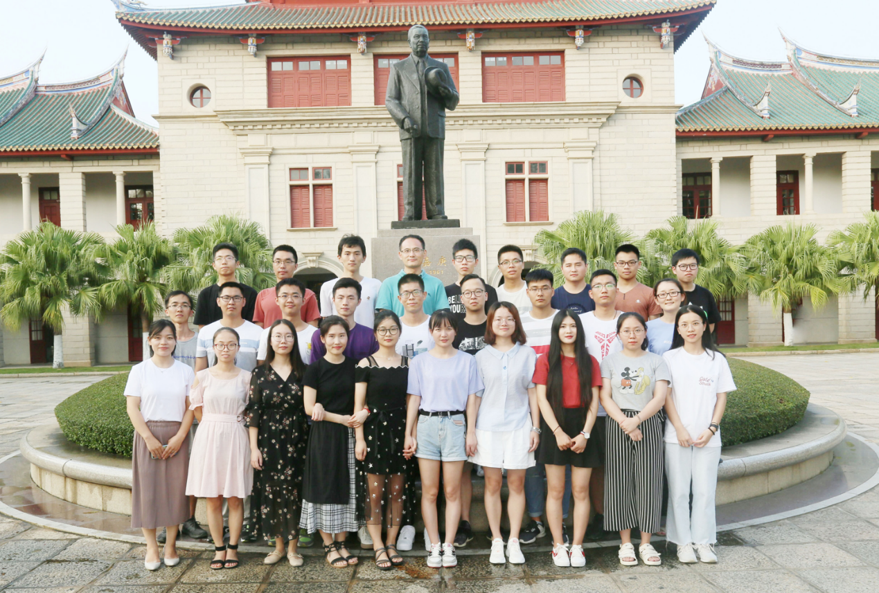
Figure: group photo of R&D team
