Paper Sharing
【International Papers】Heteroepitaxial Growth of α-Ga₂O₃ by MOCVD on a-, m-, r-, and c-Planes of Sapphire
日期:2025-08-25阅读:656
Researchers from the University of Bristol have published a dissertation titled "Heteroepitaxial Growth of α-Ga2O3 by MOCVD on a-, m-, r-, and c-Planes of Sapphire" in Crystal Growth & Design.
Background
Corundum α-Ga2O3 (space group R3̅c) boasts the widest bandgap of all Ga2O3 polymorphs (5.1–5.3 eV) and is isostructural with α-Al2O3, commonly known as sapphire. This permits not only the growth of high-quality domain-matched α-Ga2O3 layers on economical substrates (sapphire being available at significantly lower cost than native Ga2O3 substrates used for high-quality β-Ga2O3 growth) but also extensive bandgap engineering by alloying with Al over the full composition range from x = 0 to 1 in α-(AlxGa1–x)2O3, leading to a bandgap range of 5.1–8.8 eV. Such compositional control is generally more difficult in the monoclinic phase, where β-(AlxGa1–x)2O3 films typically suffer from local segregation of Al and Ga (e.g., on (001) and (2̅01) β-Ga2O3 substrates) or phase segregation of β- and γ-Ga2O3 (e.g., on (010) β-Ga2O3 substrates) toward high Al content. Up to 99% Al composition β-(AlGa)2O3 films have been achieved on (100) β-Ga2O3 substrates, but the film quality degrades with increasing Al content. In contrast, α-(AlGa)2O3 films do not degrade or even improve in crystallinity toward Al-rich regimes. Finally, it is worth highlighting that, similar to β-Ga2O3, n-type conductivity of α-Ga2O3 films can be achieved by Si, Sn, or Ge doping, with controllable carrier density over the range of 1017–1019 cm–3 and electron mobility up to 98.7 cm2 V–1 s–1 having been reported. These qualities make α-Ga2O3 an attractive material for the fabrication of high-breakdown power devices like Schottky diodes, field-effect transistors, and optoelectronic devices such as solar blind photodetectors.
Abstract
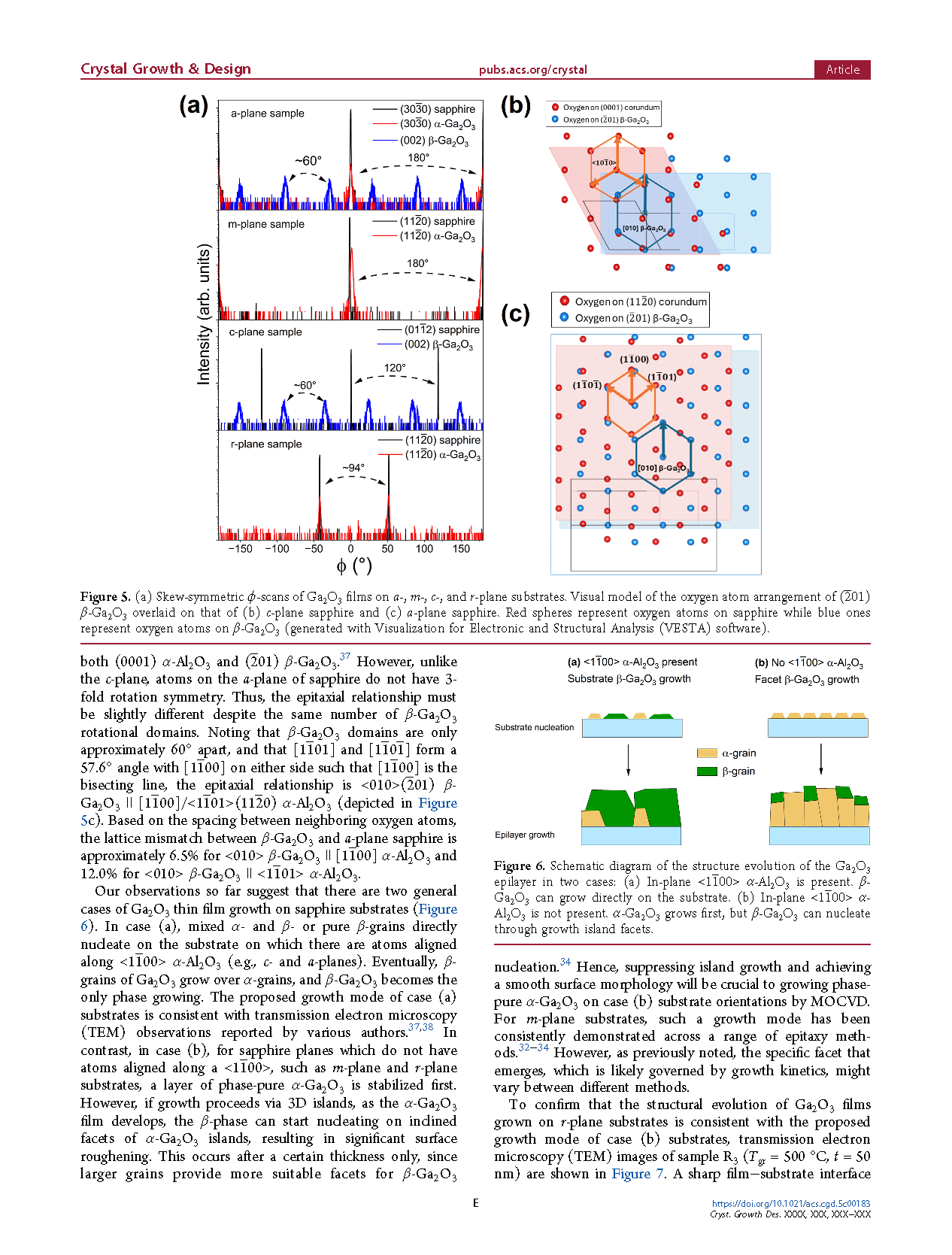
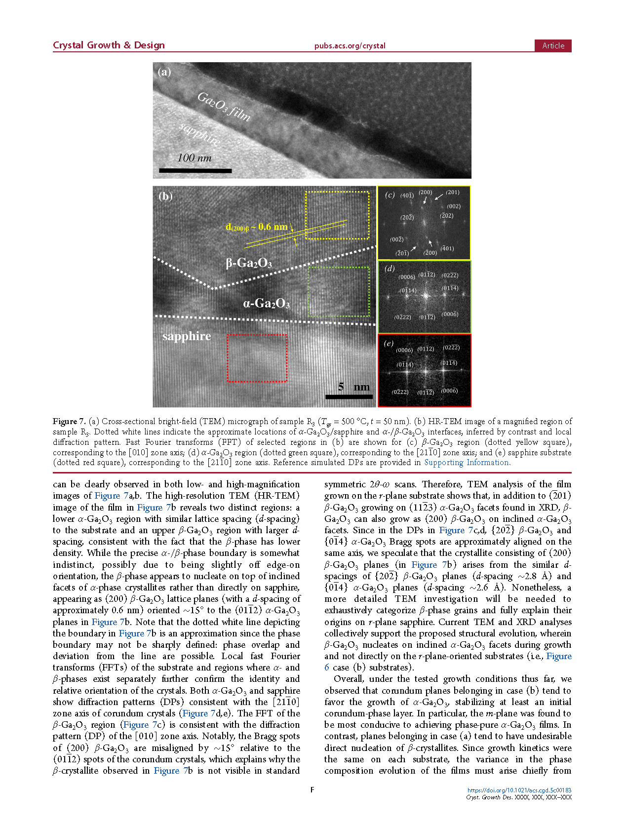
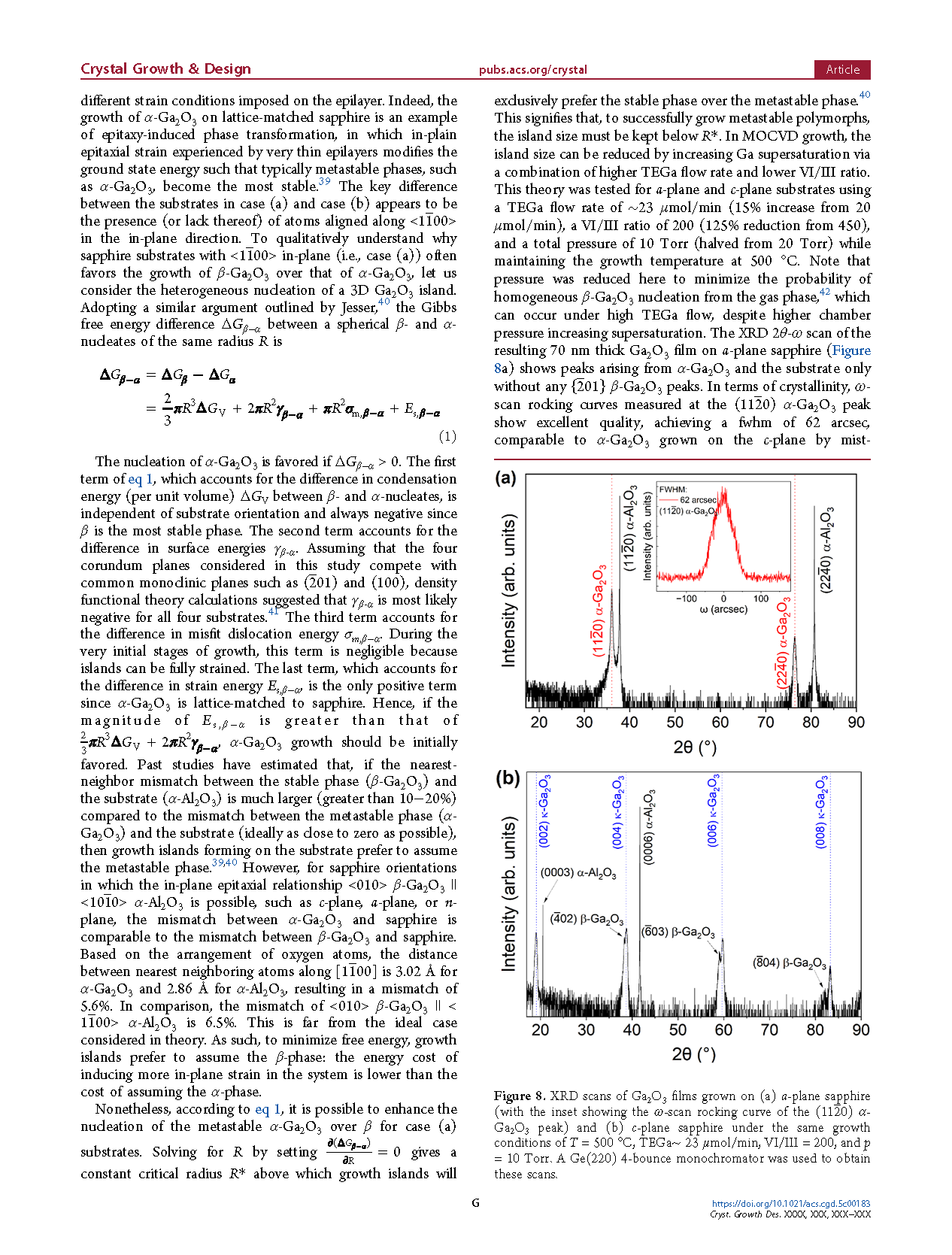
Ga2O3 thin films were deposited simultaneously on (112̅0) a-plane, (101̅0) m-plane, (0001) c-plane, and (011̅2) r-plane sapphire substrates using metal–organic chemical vapor deposition (MOCVD) and characterized by X-ray diffraction (XRD) and atomic force microscopy (AFM). The different surface energy and strain conditions imposed by each sapphire plane make the choice of substrate orientation critical to the stabilization of the α-phase. β-Ga2O3 nucleation was found to be preferential over α-Ga2O3 on sapphire orientations with <11̅00> α-Al2O3 present (c- and a-planes) when grown under the same conditions. In contrast, α-Ga2O3 is preferred during the initial stages of growth on the r- and m-plane, although suppression of island growth is required to prevent the formation of inclined facets on which β-Ga2O3 might nucleate. Transmission electron microscopy (TEM) provided a direct confirmation of this growth for r-plane substrates. Classical nucleation theory was applied to rationalize these observations and guide the search for the growth window of α-Ga2O3. As a result, decreasing the VI/III ratio and increasing the TEGa flow rate were found to be effective in realizing phase-pure α-Ga2O3 on a-plane sapphire by MOCVD with good structural quality (62 arcsec full width half-maxima of X-ray rocking curve), though the equivalent growth on c-plane substrates yielded mixed-phase β- and κ-Ga2O3─another metastable phase of Ga2O3, instead. Growth on the m-plane resulted in the smoothest surface morphology and thickest phase-pure α-Ga2O3 film, indicating that it is the most promising substrate orientation for future device manufacturing.

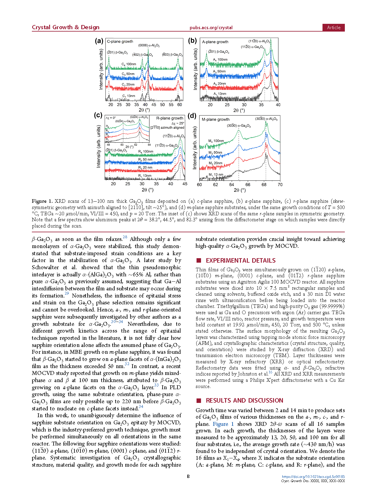
Figure 1. XRD scans of 13−100 nm thick Ga2O3 films deposited on (a) c-plane sapphire, (b) a-plane sapphire, (c) r-plane sapphire (skew-symmetric geometry with azimuth aligned to [21-10], tilt ∼25°), and (d) m-plane sapphire substrates, under the same growth conditions of T = 500 °C, TEGa ∼20 μmol/min, VI/III = 450, and p = 20 Torr. The inset of (c) shows XRD scans of the same r-plane samples in symmetric geometry. Note that a few spectra show aluminum peaks at 2θ = 38.2°, 44.5°, and 82.3° arising from the diffractometer stage on which samples were directly placed during the scan.

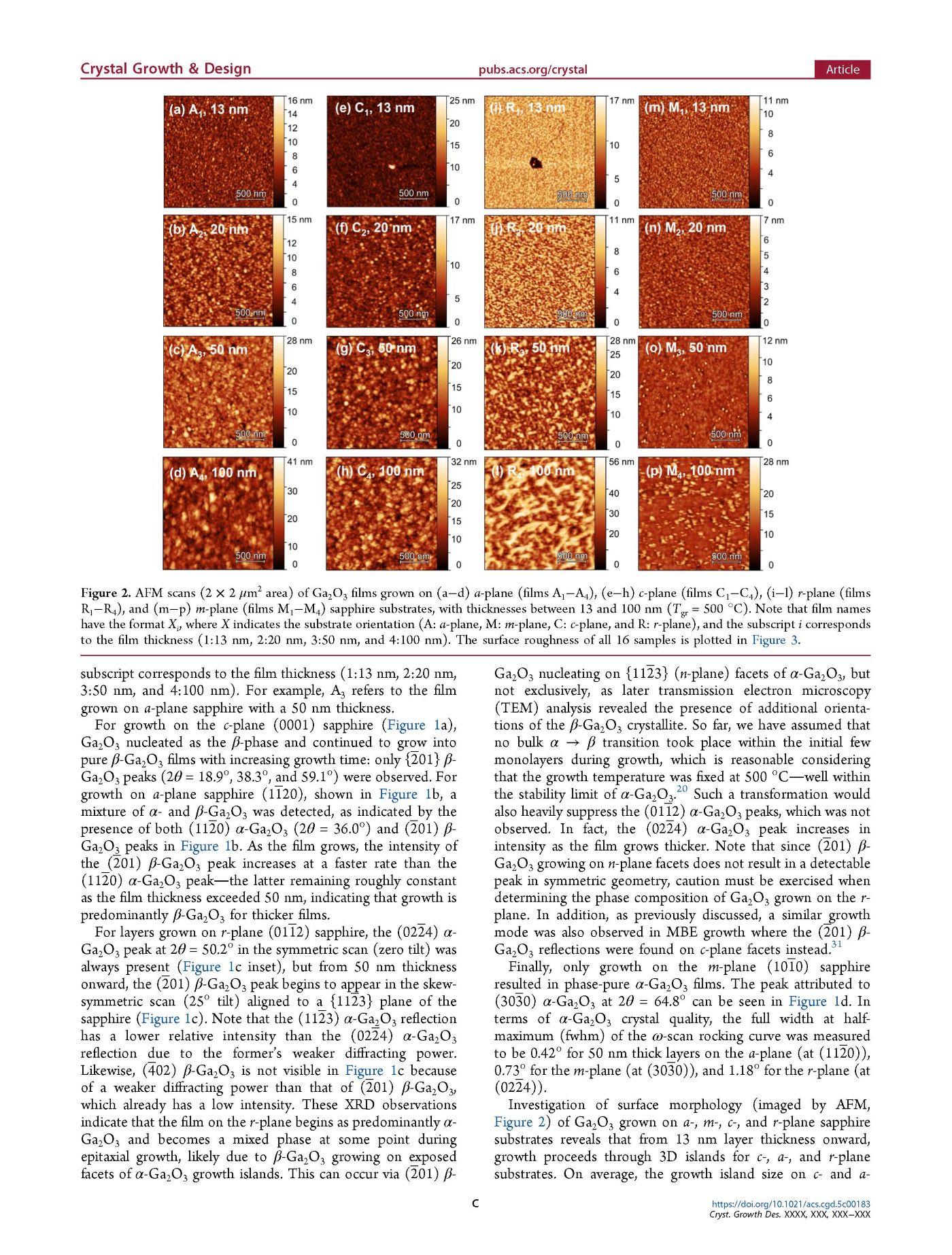
Figure 2. Schematic diagram of the structure evolution of the Ga2O3 epilayer in two cases: (a) In-plane α-Al2O3 is present. Β-Ga2O3 can grow directly on the substrate. (b) In-plane α-Al2O3 is not present. α-Ga2O3 grows first, but β-Ga2O3 can nucleate through growth island facets.
DOI:
doi.org/10.1021/acs.cgd.5c00183