


Member News
【Member News】Qi Hongji, Chairman of Fujia Gallium, Speaks at IPF2025 on Advances in Gallium Oxide Single Crystal Substrates and Epitaxial Technologies
日期:2025-08-26阅读:874
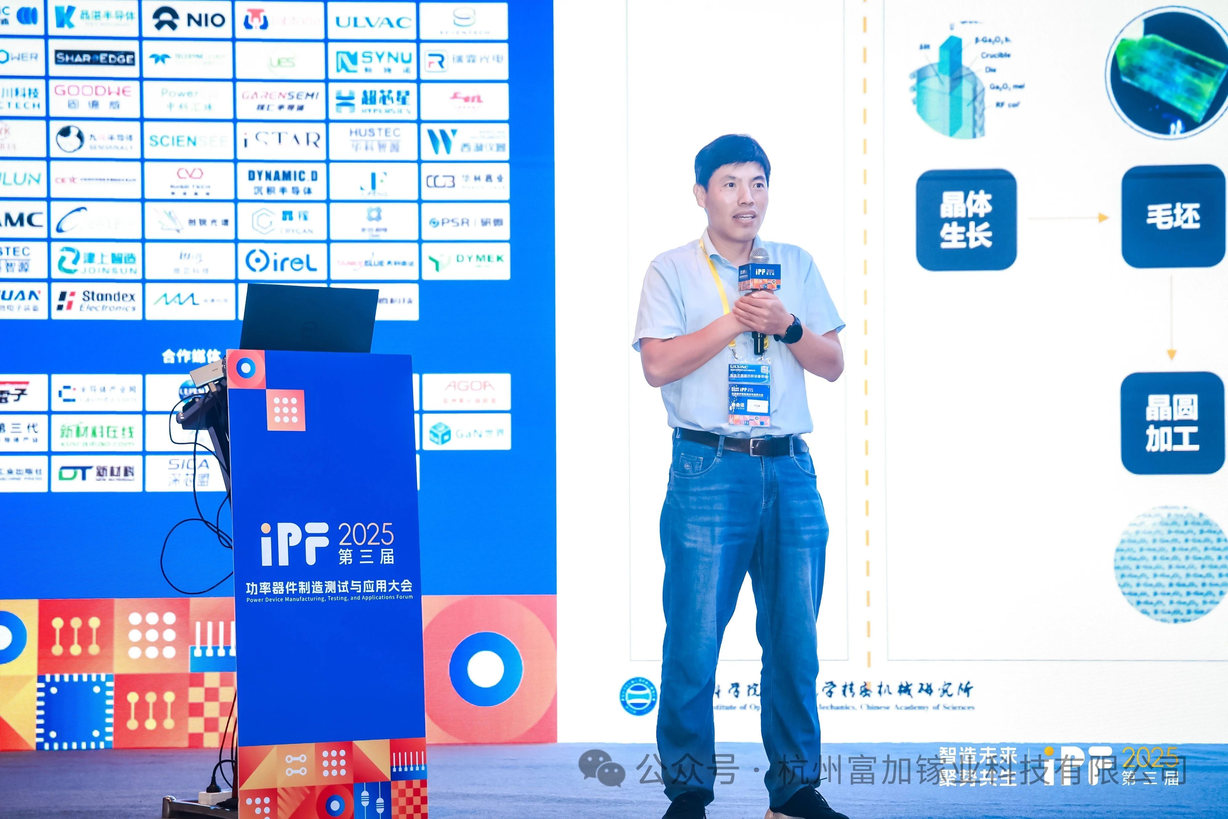
The third Power Device Manufacturing, Testing, and Applications Forum (IPF 2025) kicked off grandly at Radisson Blu Resort Wuxi Lianghong Wetland on August 21-22, 2025. The conference spotlighted the intelligent transformation of power semiconductors and collaborative innovation across the entire industry chain, bringing together leading global experts to discuss breakthrough technological advances.
As a leading enterprise in the ultra-wide band gap semiconductor Gallium Oxide field, Hangzhou Fujia Gallium Technology Co., LTD. (hereinafter referred to as "Fujia Gallium") was invited to attend the conference. Qi Hongji, the company's chairman, delivered a significant report at the sub-forum on "Technological Development of Next-Generation High-Efficiency Power Semiconductors". The report points out that in the field of Gallium Oxide, China has the advantages of raw materials and market scale. In order to achieve the integration of the Gallium Oxide industrial chain as soon as possible, it is necessary to strengthen the technological research and development and industrialization of single crystal, epitaxial, device and related equipment. The report shares the practical achievements and industrial vision of Fujia Gallium. In addition, the construction of the industrial chain requires strong support from social organizations such as associations and alliance. The Ultra-Wide Band Gap Semiconductor Alliance, which was established in Shanghai in May 2025, will play a significant role. The 5th Cross-Strait Conference on Gallium Oxide and Related Materials and Devices(CSGO), which is scheduled to be held from October 10th to 12th, also provides an excellent communication platform for sharing research achievements in the field of Gallium Oxide.
Deepening the Full Industrial Chain Layout,
Strengthening the Foundation for Gallium Oxide Industrialization
From "material breakthroughs" to "device implementation", the full industrial chain capability is the core driver for Gallium Oxide technology from the laboratory to the market. At the beginning of the report, Dr. Qi Hongji underscored the importance of industrial chain layout. Since its establishment in 2019, Fujia Gallium has been committed to the vision of "Enabling the World to Use High-Quality Materials", continuously breaking through key technical bottlenecks of Gallium Oxide. It has now built a full-chain industrialization system covering "equipment - substrate - epitaxial - device verification", and has become one of the few domestic enterprises to achieve dual independent control over Gallium Oxide materials and equipment.
At the core product end, Fujia Gallium has realized mass production of 6-inch Gallium Oxide single crystal substrates, with products reaching the industrialization threshold of semiconductor device process lines. The 4-inch MOCVD homoepitaxial wafer has excellent performance, achieving an epitaxial film thickness exceeding 10 μm and carrier mobility above 180 cm²/V·s. Across 6-inch wafers, thickness uniformity is stably controlled within ±2%, providing highly adaptable fundamental materials for downstream power device manufacturing. Meanwhile, the company’s independently developed Gallium Oxide EFG and VB equipment not only support crystal growth from 2 to 6 inches, but also take the lead in realizing intelligent “one-click crystal growth” operation, effectively addressing the equipment bottleneck for Gallium Oxide industrialization.
Currently, Fujia Gallium is accelerating the construction of its 6-inch Gallium Oxide single crystal and epitaxial wafer production lines. Looking ahead, the company aims to reach an annual capacity of 10,000 wafers, further bridging the “material–device–application” chain and delivering high-efficiency semiconductor solutions for photovoltaics, energy storage, new energy vehicles, and other sectors.
Taking the Lead in the UWBG Semiconductor Alliance,
Co-Creating an Ecosystem of Industrial Synergy
The development of the Gallium Oxide industry cannot do without cross-field and cross-sector collaborative innovation. Dr. Qi Hongji emphasized in his report that Fujia Gallium, as one of the founding members of the Ultra-Wide Band Gap Semiconductor Innovation and Development Alliance, has consistently been actively promoting the integration of alliance resources and the deep collaboration across industry, academia, research, and applications.
This alliance brings together top domestic research institutions, leading manufacturing enterprises, financial investment bodies, and other key stakeholders, focusing on cutting-edge technology R&D, standard setting, talent cultivation, and the industrialization of ultra-wide band gap semiconductors. Leveraging the alliance platform, Fujia Gallium has established collaborations with numerous downstream device manufacturers, universities, and research institutions to jointly develop Gallium Oxide-based devices such as SBDs (Schottky Barrier Diodes) and MOSFETs (metal–oxide–semiconductor field-effect transistors). Currently, the performance of SBD devices based on the company’s conductive substrates and epitaxial wafers approaches the theoretical limits of Silicon Carbide devices. In addition, the tape-out of 4-inch epitaxial wafers has been successfully completed.
“The value of the alliance lies in ‘breaking boundaries’—overcoming technological barriers, corporate boundaries, and resource silos,” said Dr. Qi Hongji. Looking ahead, Fujia Gallium will continue to use the alliance as a platform to promote technology sharing across upstream and downstream enterprises, jointly establish industry standards, and accelerate the development of the Gallium Oxide industry from isolated breakthroughs to clustered, large-scale growth.
Notice of the CSGO
Creating a New Platform for International Exchange
To further connect global innovative resources in the Gallium Oxide field, the 5th5th Cross-Strait Conference on Gallium Oxide and Related Materials and Devices(CSGO), hosted by the Shanghai Key Laboratory of Wide Band Gap and Ultra-Wide Band Gap Semiconductor Materials, will be held at the Songshan Lake Laboratory in Dongguan, Guangdong Province from October 10th to 12th, 2025. The conference aims to provide a high-level communication platform for experts, scholars, enterprise representatives, and investment institutions in the Gallium Oxide field across Asia and worldwide.
The conference will focus on core topics such as Gallium Oxide single crystal growth, epitaxial technology, device design and fabrication, and the expansion of application scenarios. It will include keynote presentations, technical discussions, and achievement exhibitions, among other sessions, to explore global Gallium Oxide technology pathways and market opportunities. “Through this conference, we hope to showcase China’s achievements in Gallium Oxide technology to the world, while also leveraging global resources to support the development of China’s industry,” said Qi Hongji. He added that Fujia Gallium will share its latest research and development achievements and industrialization experience at the conference, and looks forward to collaborating with all parties to promote Gallium Oxide as a core material for next-generation power semiconductors. “
Live Interaction Fever
Fujia Gallium’s Flagship Products Draw Attention
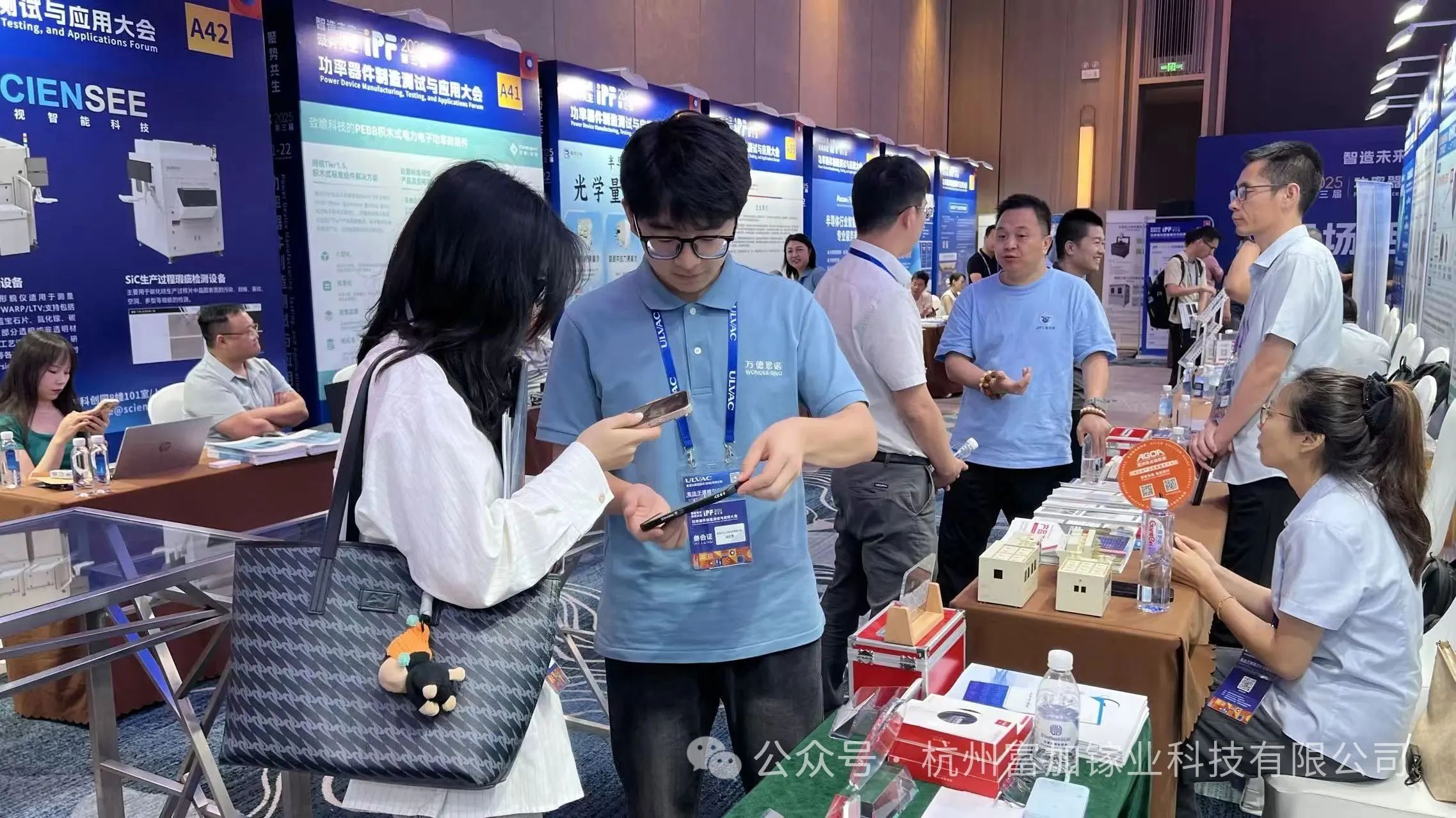
In addition to the report sharing, Fujia Gallium Industry set up a dedicated booth at A30 in Area A of the conference, including 6-inch Gallium Oxide wafers, 4-inch Gallium Oxide epitaxial wafer, and EFG/VB crystal growth equipment. During the exhibition, many attendees stopped by the booth to consult and exchange ideas, highly recognizing the technical strength and industrialization progress of Fujia Gallium, and many downstream enterprises expressed interest in potential cooperation.
Fujia Gallium’s appearance at the IPF2025 not only served as a concentrated showcase of its Gallium Oxide technology achievements, but also demonstrated the company’s determination to promote industrial collaboration and connect global resources. Looking ahead, Fujia Gallium will continue to focus on the ultra-wide band gap semiconductor field, with technological innovation at its core, industrial chain collaboration as its support, and international exchange as its bridge, helping China’s Gallium Oxide industry leap from “following” to “leading” and contributing Chinese strength to the development of high-efficiency power semiconductors worldwide.
Product Introduction
Equipment:
The company has developed the world's first EFG equipment equipped with "one-click crystal growth", which can meet the growth requirements of 2-6-inch crystals. Currently, it has obtained 6 domestic authorized patents and 4 international granted patents, and can provide equipment and complete process packages.
The company has independently developed fully automated VB crystal growth systems, becoming the first in China to break through the technical bottleneck of 4-inch single crystal growth and achieve the production of large-size VB single crystals. It currently holds 6 granted domestic patents and 4 granted international patents, and can supply VB equipment along with complete process packages tailored to customer requirements.
Considering the brittleness and easy-cleavage characteristics of gallium oxide, the company has also developed 2–6 inch gallium oxide single crystal substrate grinding and polishing systems. Mature grinding, polishing, and cleaning process packages are available upon request.
Single Crystal and Epitaxial Wafer:
The company has established two enterprise standards and obtained ISO9001 quality management system certification. It supplies the market with various crystal orientation Gallium Oxide single crystal substrates ranging from 10mm to 6 inches, MOCVD-grown Gallium Oxide epitaxial wafer ranging from 10mm to 4 inches, and 10mm MBE-grown Gallium Oxide epitaxial wafer.
About Fujia Gallium
Hangzhou Fujia Gallium Technology Co., LTD., founded on December 31, 2019, is the first "hard technology" enterprise registered by Hangzhou Institute of Optics and Fine Mechanics. With the vision of "Making the World Use Good Materials", the company focuses on the industrialization work of wide bandgap semiconductor Gallium Oxide materials. The core products include Gallium Oxide single crystal substrates, MOCVD epitaxial wafers, MBE epitaxial wafers, Gallium Oxide crystal growth and processing equipment. The products mainly serve the fields of power devices, microwave and radio frequency, and optoelectronic detection. The company's series of important achievements in the development of Gallium Oxide have been featured and reported by well-known media such as People's Daily, Xinhuanet, China Securities News, and The Paper.
At present, the company has won a number of honors: In 2022, it won the Zhejiang Province Science and Technology Small and Medium-Sized Enterprise; National High-Tech Enterprise in 2023; In 2024, it will be awarded as Hangzhou Enterprise High-Tech Research and Development Center and Zhejiang Special Small and Medium-Sized Enterprise. Obtain ISO9001 quality system certification in 2025 (No. 20225Q20294R0M); It undertook one Gallium Oxide project for the National Development and Reform Commission and participated in three national and provincial projects from the Ministry of Science and Technology, Zhejiang Province, and Shanghai. In addition, it has obtained 12 international patents authorized (6 in the United States and 6 in Japan), 40 domestic patents authorized, 3 trademark certification and registration of "Fujia Gallium", and 4 software copyrights (crystal growth control software of "one-click crystal growth").
