Paper Sharing
【Domestic Papers】High-performance Type-Ⅰ Sn-doped-Ga₂O₃/SnSe₂ Heterojunction Photodetectors Enabled by Fowler-Nordheim Tunneling
日期:2025-08-29阅读:633
Researchers from the South China Normal University have published a dissertation titled "High-performance Type-Ⅰ Sn-doped-Ga2O3/SnSe2 Heterojunction Photodetectors Enabled by Fowler-Nordheim Tunneling" in Applied Physics Letters.
Project Support
This work was supported by the National Natural Science Foundation of China (No. 62474165, 11974122 and U22A2073), Science and Technology Major Project of Henan Province (231100230300), the Foundation of National Key Laboratory of Plasma Physics (Grant No. 6142A04240204), Henan Association for Science and Technology Youth Talent Support Program (2024HYTP024) and the Scientific Research Innovation Project of Graduate School of South China Normal University.
Abstract
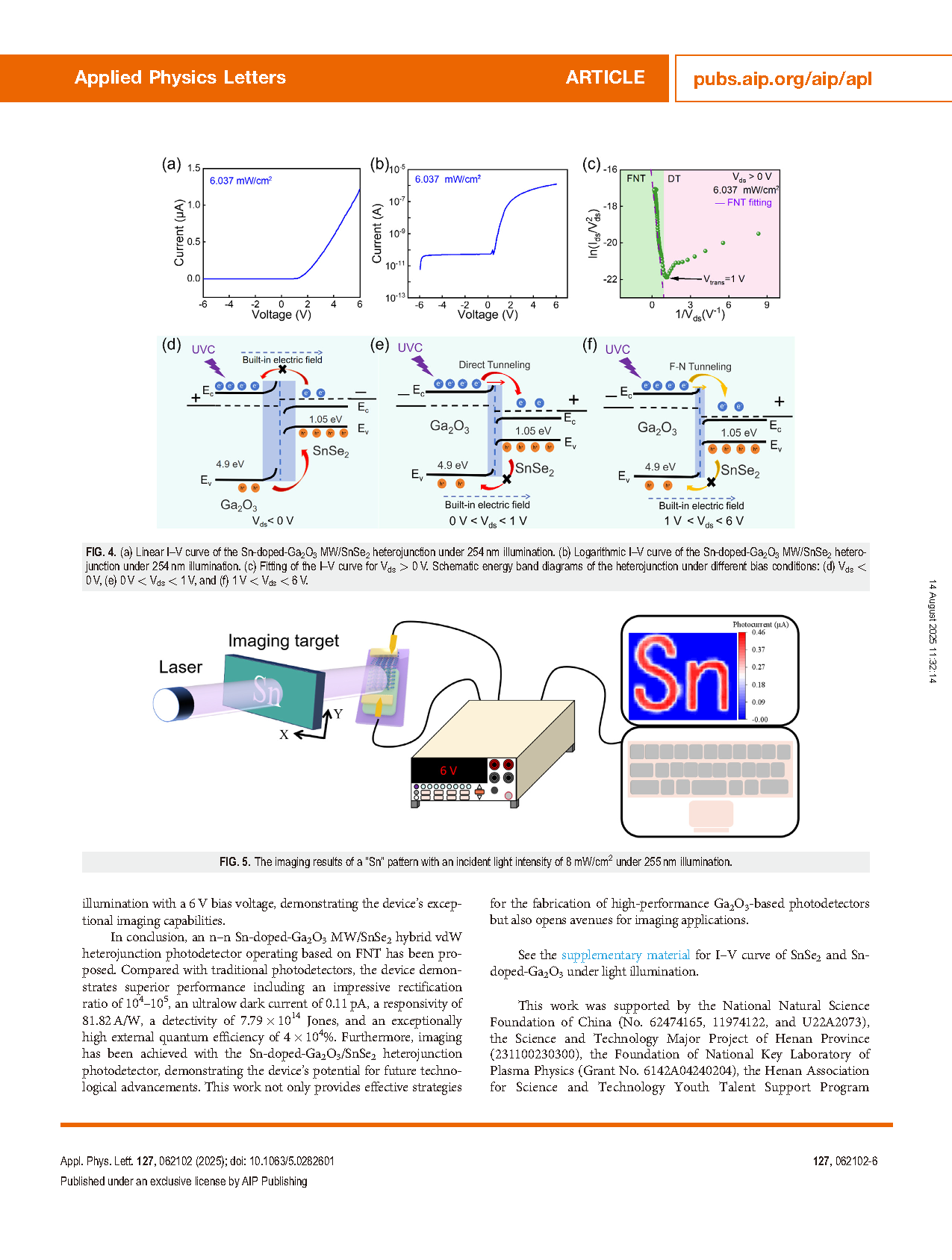
Gallium oxide (Ga2O3) is renowned for its exceptional physical and chemical properties, making it an ideal material for solar-blind photodetectors. In this study, Sn-doped-Ga2O3 microwires (MWs) were utilized to fabricate a type-I heterojunction photodetector with SnSe2. The Sn-doped-Ga2O3 MW/SnSe2 hybrid van der Waals heterojunction exhibits both direct tunneling and Fowler–Nordheim tunneling under positive voltages. By exploiting the Fowler–Nordheim tunneling mechanism at a 6 V bias, the device demonstrates outstanding performance under 254 nm illumination, achieving a rectification ratio of 104–105, an ultralow dark current of 0.11 pA, a responsivity of 81.82 A/W, a detectivity of 7.79 × 10¹⁴ Jones, and an exceptionally high external quantum efficiency of 4 × 10⁴%. These impressive characteristics make the heterojunction photodetector highly suitable for high-quality imaging applications. This research offers a promising processing solution for Ga2O3-based optoelectronic devices, further extending their potential for versatile solar-blind detection and imaging applications.
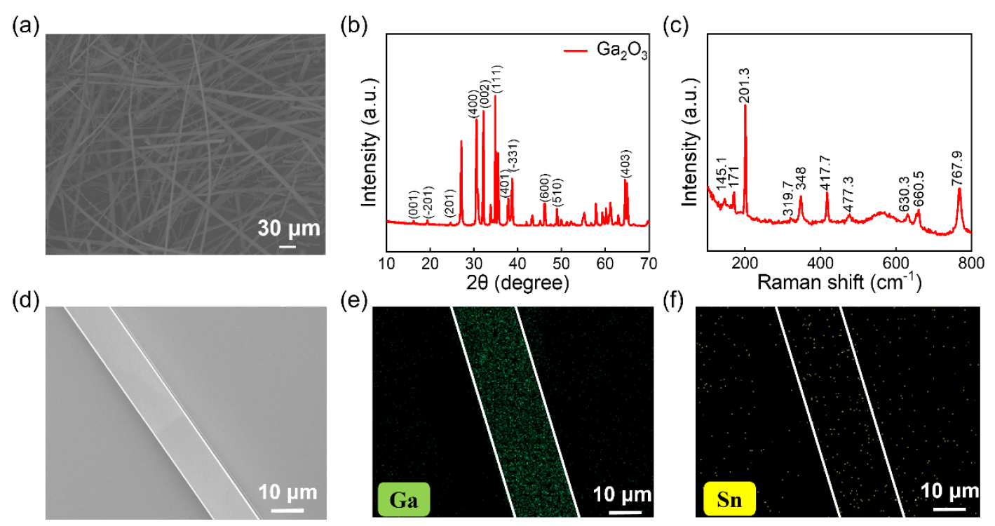
Figure 1 Basic characterization of Sn-doped-Ga2O3 MW
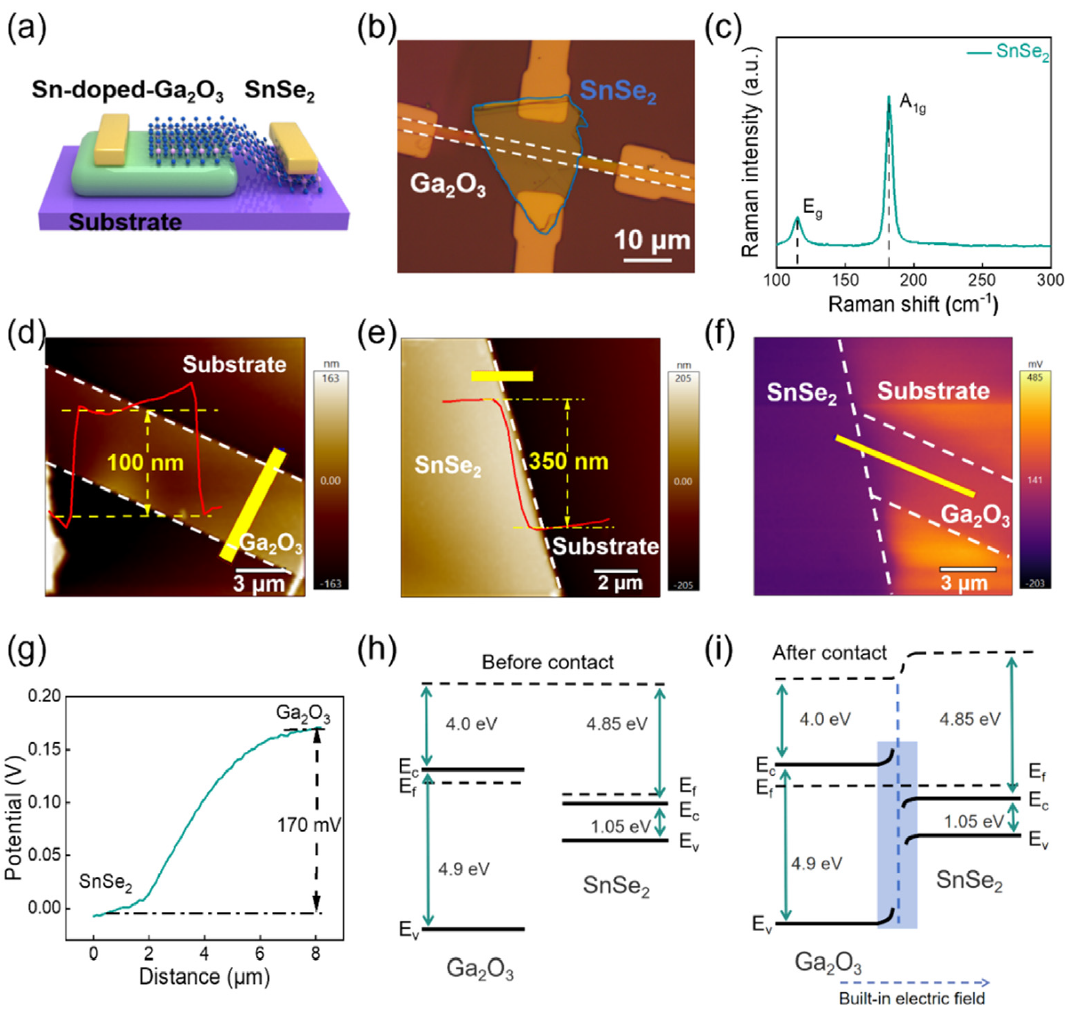
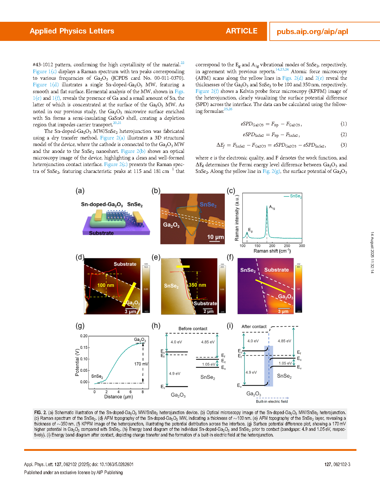
Figure 2 Schematic diagram of the structure, basic characterization, and band diagram of Sn-doped-Ga2O3 MW/SnSe2 heterojunction device.
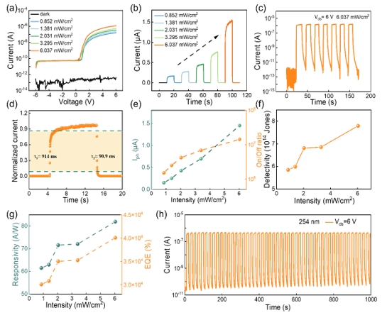
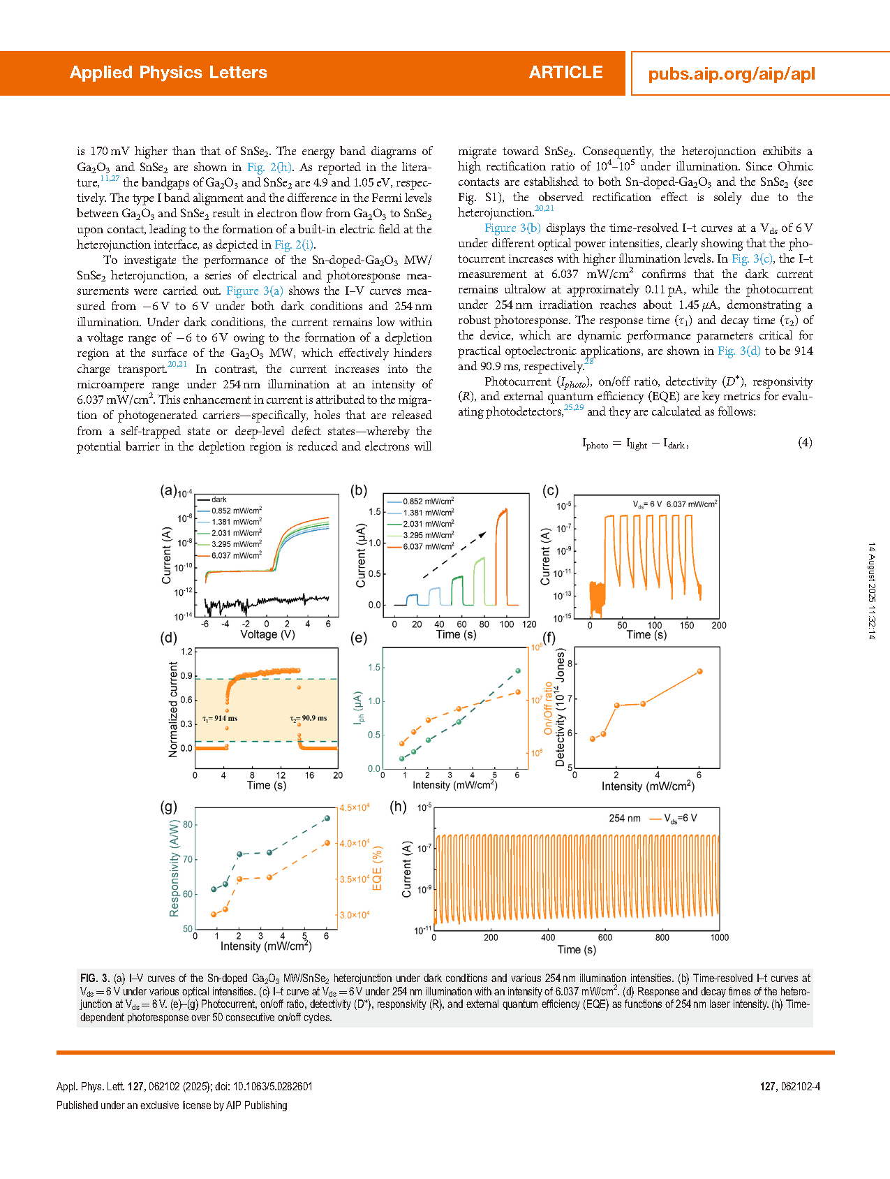
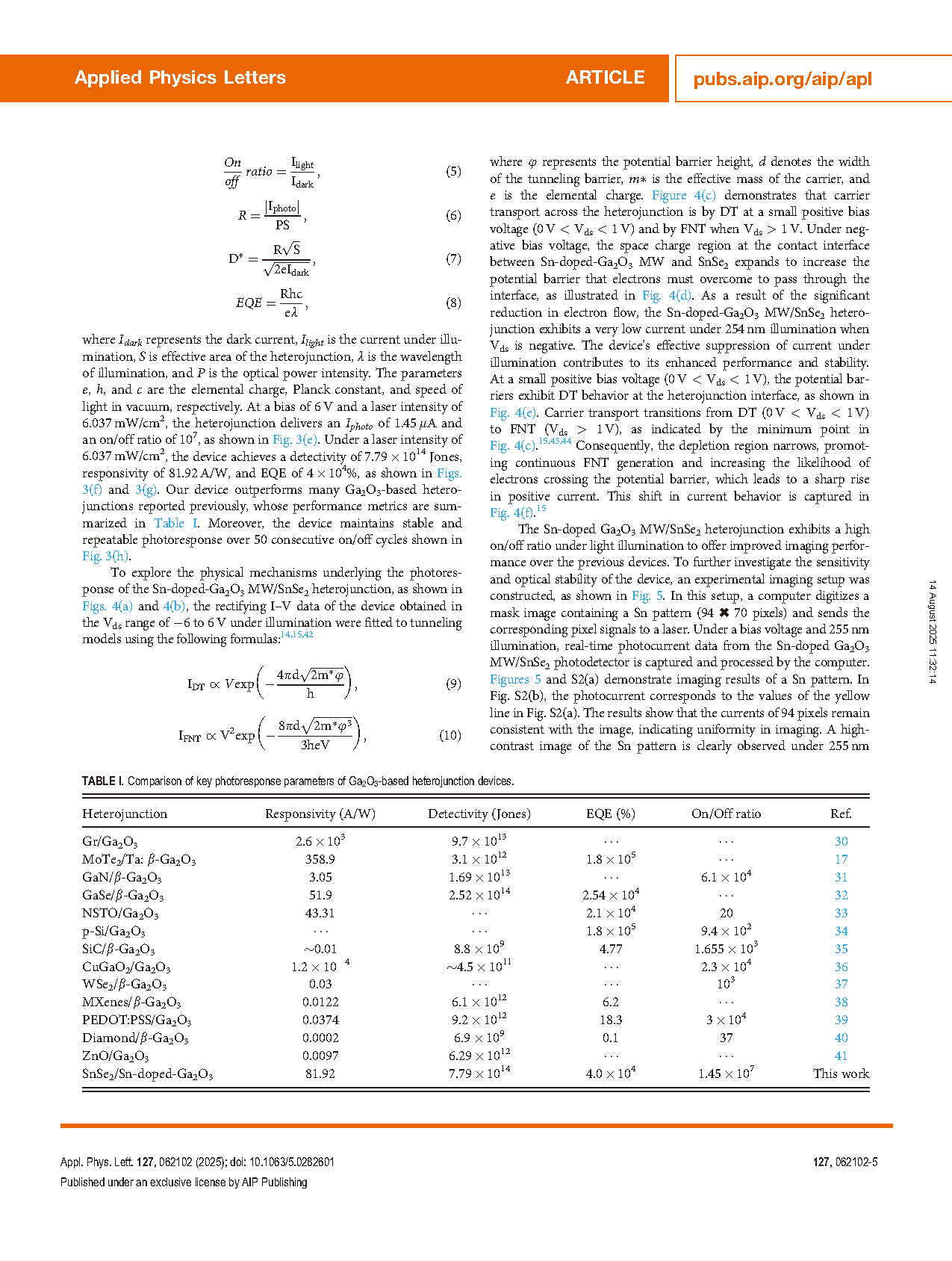
Figure 3 Optoelectronic Performance of Sn-doped-Ga2O3 MW/SnSe2 Heterojunction Device
DOI:
doi.org/10.1063/5.0282601