Paper Sharing
【International Papers】Near-ideal vertical β-Ga₂O₃ Schottky diode reverse leakage current via sputtered ultra-high-κ BaTiO₃dielectric field-management
日期:2025-09-01阅读:634
Researchers from the Wright-Patterson Air Force Base have published a dissertation titled "Near-ideal vertical β-Ga2O3 Schottky diode reverse leakage current via sputtered ultra-high-κ BaTiO3 dielectric field-management" in APL Electronic Devices.
Background
Vertical β-Ga2O3 diodes are of interest for power applications due to the potential scaling and efficiency benefits enabled by their wide bandgap of 4.8 eV and expected critical field strength of 8 MV/cm. Baliga’s Figure of Merit (BFOM) predicts unipolar power devices have the potential to outperform Si, SiC, and GaN power devices. The availability of homoepitaxial growth on high-quality melt-grown substrates could offer potential cost benefits over other technologies as well. Recently, device research has accelerated, with the goal of realizing the potential efficiency benefits indicated by figures of merit. Schottky barrier diodes (SBDs) are of interest in power switching applications due to their improved reverse recovery time over p-n diodes. β-Ga2O3 SBDs have been demonstrated on a variety of substrates and via several growth methods, including halide vapor phase epitaxy (HVPE) and metal-organic chemical vapor deposition (MOCVD). SBDs with no field management are limited by field crowding at the anode edge, which leads to a local increase in leakage current, causing early breakdown. However, with no shallow p-type dopants, typical power device field management strategies with p-n homojunctions are not feasible for β-Ga2O3. As an alternative, p-n heterojunctions using p-Si and p-NiO have been shown to successfully achieve reduced leakage and increased breakdown voltage when implemented as p-n diodes or junction termination extension structures. However, to avoid being field-limited by narrower bandgap materials and to avoid switching penalties of p-type materials, unipolar edge termination structures are beneficial.
Abstract
We report the use of ultra-high-κ BaTiO3 films deposited via RF sputtering for field management in vertical β-Ga2O3 Schottky barrier diodes. The reverse leakage current for field-plated devices with varying oxide thickness is compared to a theoretical 1-D reverse leakage current that includes thermionic emission with image-force lowering (IFL) and tunneling current. We find near-ideal agreement in leakage current with a thin BaTiO3 field oxide layer and slight deviation from the modeled current as the BaTiO3 gets thicker due to enhanced field-crowding at the anode edge. The effect of increasing BaTiO3 layer thickness on increased field at the anode edge is validated using a Silvaco Victory Device TCAD model. In addition, we show that for a device operating temperature of 150 °C, the measured reverse characteristics deviate substantially from the theoretical leakage, presumably due to thermally excited electron emission over the 80 meV band offset between BaTiO3 and β-Ga2O3. Finally, we demonstrate an Al2O3 interlayer with the BaTiO3 to decrease thermally induced leakage. The mitigation of thermal electron emission improves the agreement between measured and theoretical leakage at 150 °C. These results show the efficacy of a high-κ dielectric field-management layer in vertical β-Ga2O3 devices, which will be critical due to the absence of shallow p-type dopants in β-Ga2O3. This provides a path forward to realizing the potential of β-Ga2O3 power devices.
Conclusion
We have demonstrated near-ideal reverse leakage current in vertical β-Ga2O3 Schottky barrier diodes via field plates using ultrahigh-κ sputtered BaTiO3 as a field plate oxide. We showed good agreement between measured reverse leakage characteristics and theoretical 1-D reverse leakage current, calculated by determining the theoretical total thermionic emission with image force lowering and tunneling current at high fields. We found near-ideal agreement with a thin BaTiO3 (40 nm) field-management layer, with measured J–F characteristics diverging slightly from the modeled leakage as the BaTiO3 became thicker (110 and 320 nm) due to field crowding at the anode edge of the device shown in Silvaco Victory Device TCAD modeling. In addition, we showed a MOSCAP with a 4.1 MV/cm average surface field. We demonstrated that the devices deviate substantially from the leakage model at 150 °C due to thermally excited electron emission of the small band offset between BaTiO3 and Ga2O3. This can be mitigated via the inclusion of a wide-bandgap dielectric interlayer, also demonstrated in this study. This provides a path forward for dielectric field-management in vertical Ga2O3 devices, which will be critical to realizing β-Ga2O3’s theoretical performance in the absence of traditional field-management techniques enabled by shallow p-type dopants.

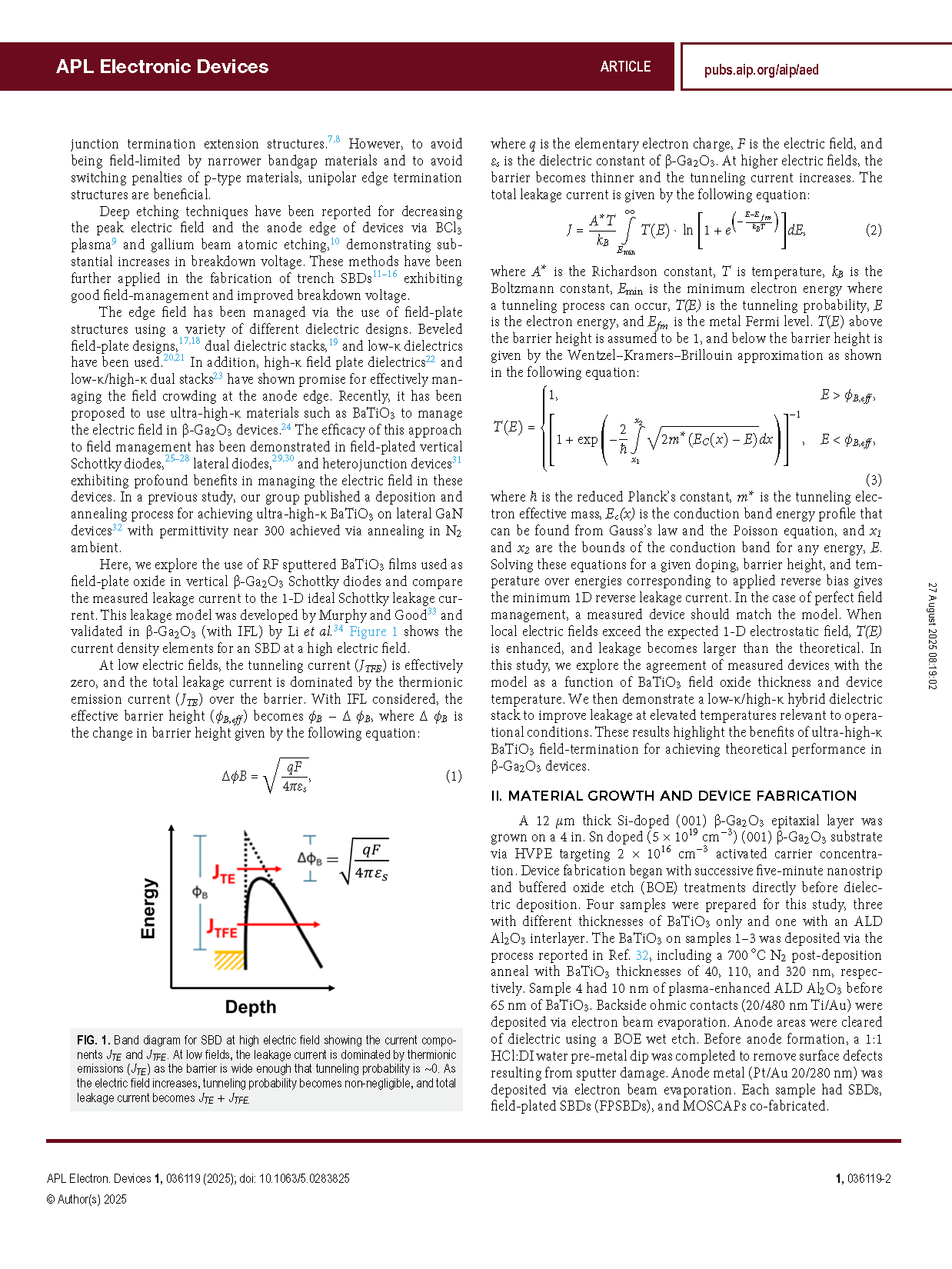
FIG. 1. Band diagram for SBD at high electric field showing the current components JTE and JTFE. At low fields, the leakage current is dominated by thermionic emissions (JTE) as the barrier is wide enough that tunneling probability is ∼0. As the electric field increases, tunneling probability becomes non-negligible, and total leakage current becomes JTE + JTFE.
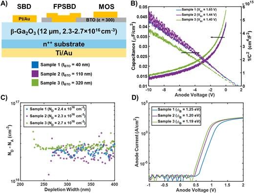
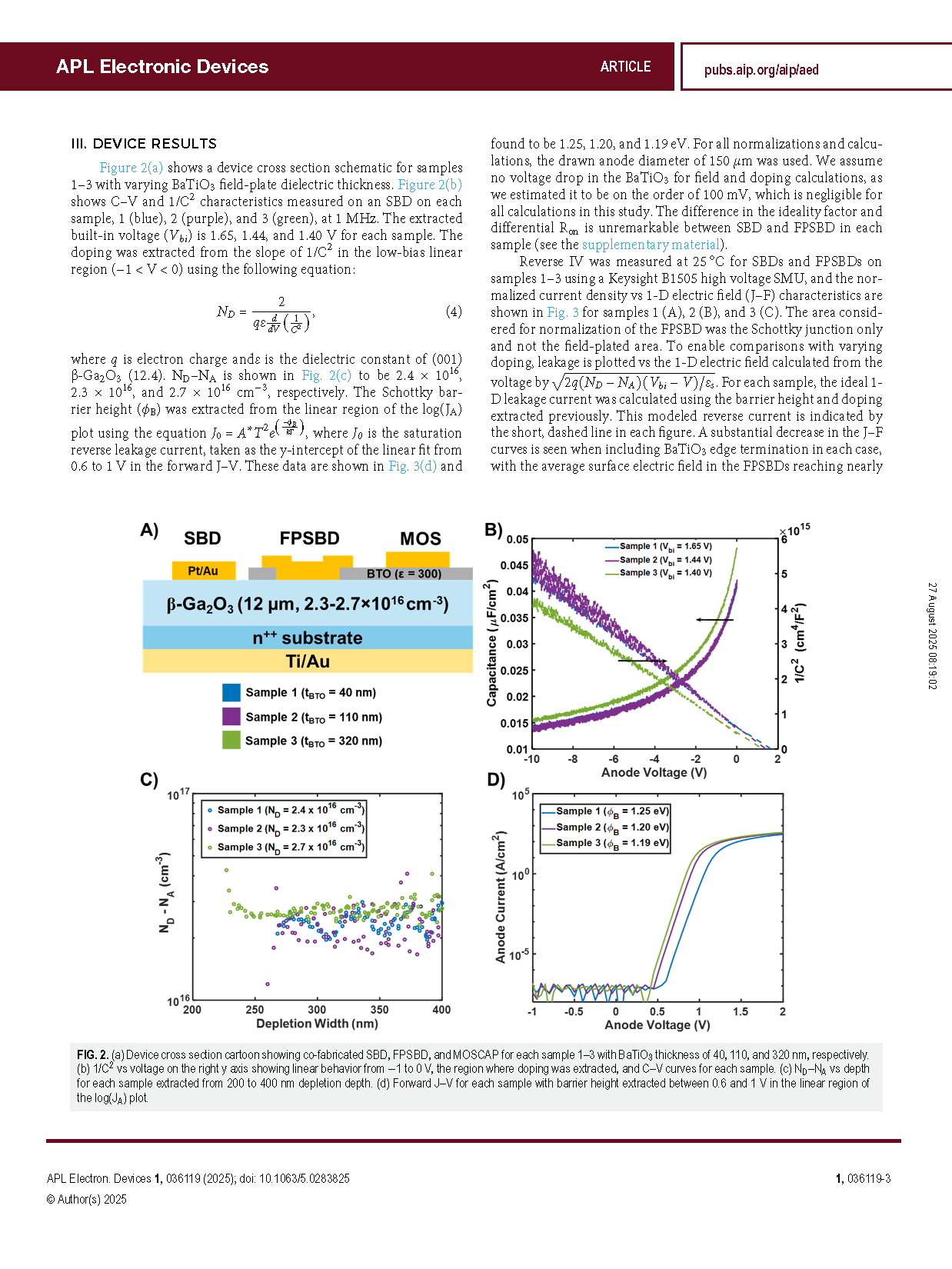
FIG. 2. (a) Device cross section cartoon showing co-fabricated SBD, FPSBD, and MOSCAP for each sample 1–3 with BaTiO3 thickness of 40, 110, and 320 nm, respectively. (b) 1/C2 vs voltage on the right y axis showing linear behavior from −1 to 0 V, the region where doping was extracted, and C–V curves for each sample. (c) ND–NA vs depth for each sample extracted from 200 to 400 nm depletion depth. (d) Forward J–V for each sample with barrier height extracted between 0.6 and 1 V in the linear region of the log(JA) plot.
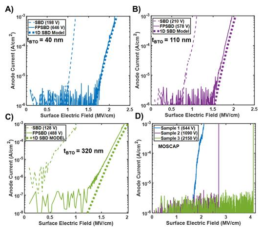
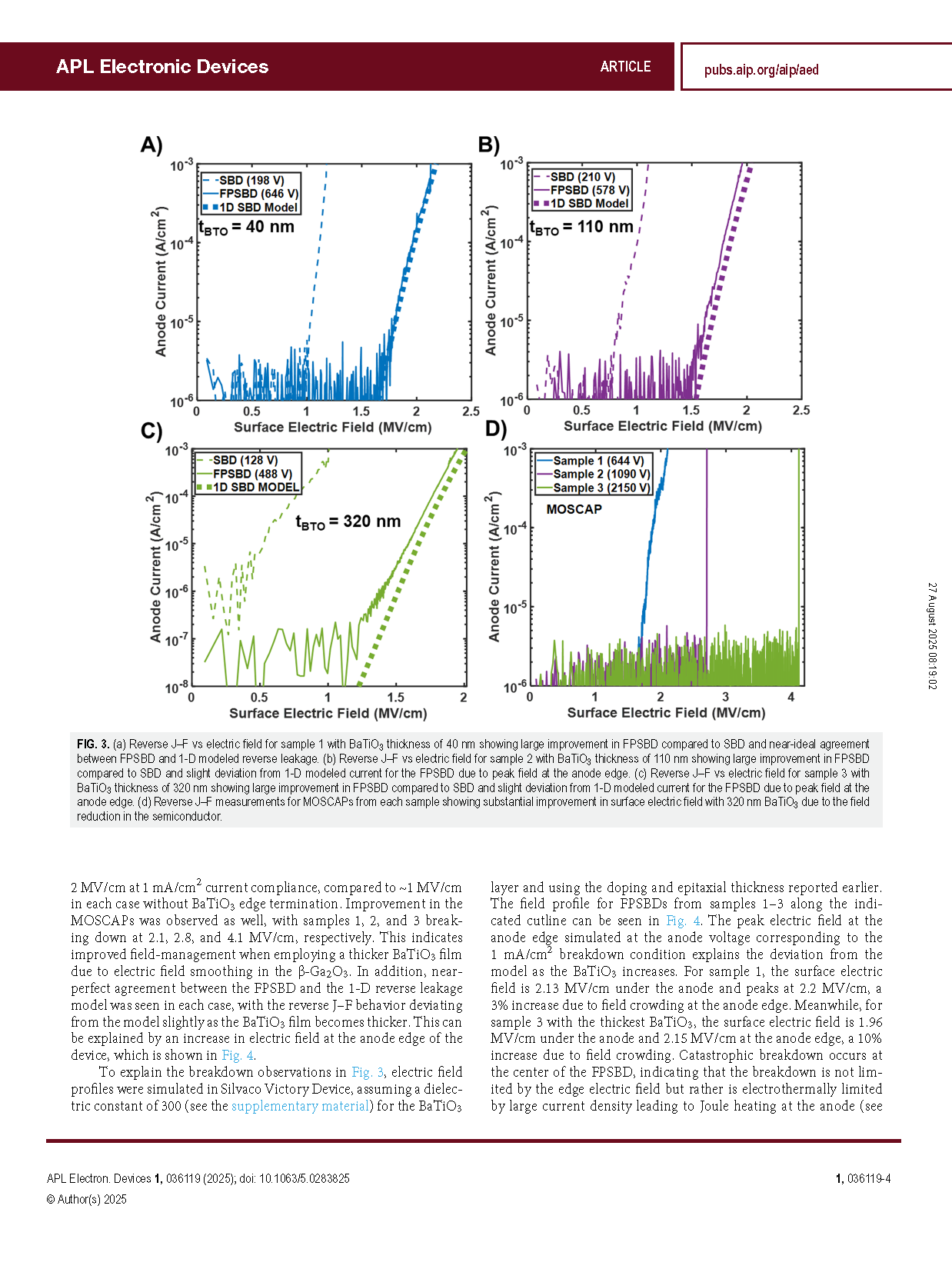
FIG. 3. (a) Reverse J–F vs electric field for sample 1 with BaTiO3 thickness of 40 nm showing large improvement in FPSBD compared to SBD and near-ideal agreement between FPSBD and 1-D modeled reverse leakage. (b) Reverse J–F vs electric field for sample 2 with BaTiO3 thickness of 110 nm showing large improvement in FPSBD compared to SBD and slight deviation from 1-D modeled current for the FPSBD due to peak field at the anode edge. (c) Reverse J–F vs electric field for sample 3 with BaTiO3 thickness of 320 nm showing large improvement in FPSBD compared to SBD and slight deviation from 1-D modeled current for the FPSBD due to peak field at the anode edge. (d) Reverse J–F measurements for MOSCAPs from each sample showing substantial improvement in surface electric field with 320 nm BaTiO3 due to the field reduction in the semiconductor.
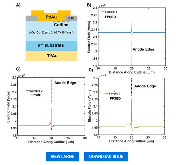
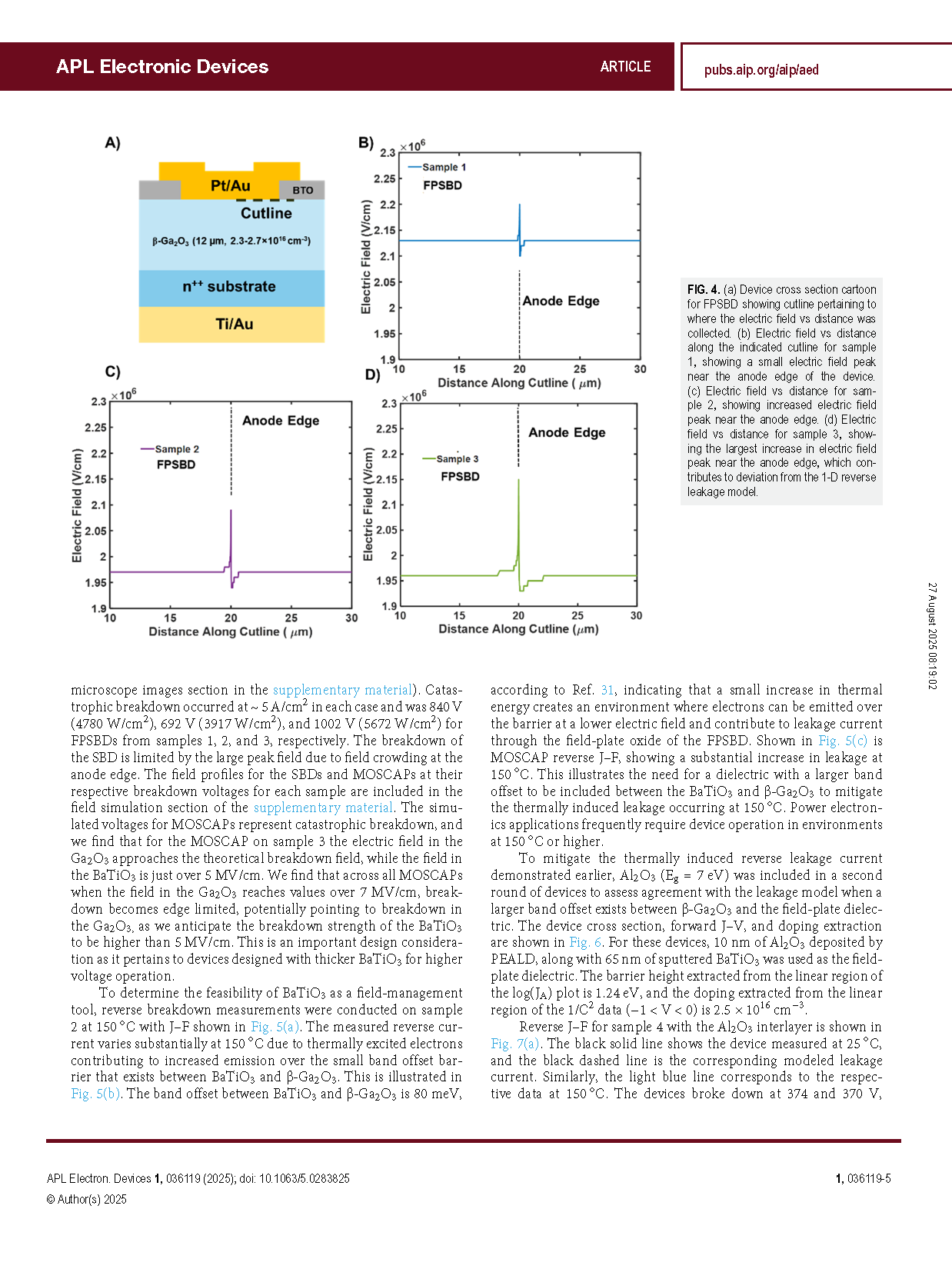
FIG. 4. (a) Device cross section cartoon for FPSBD showing cutline pertaining to where the electric field vs distance was collected. (b) Electric field vs distance along the indicated cutline for sample 1, showing a small electric field peak near the anode edge of the device. (c) Electric field vs distance for sample 2, showing increased electric field peak near the anode edge. (d) Electric field vs distance for sample 3, showing the largest increase in electric field peak near the anode edge, which contributes to deviation from the 1-D reverse leakage model.
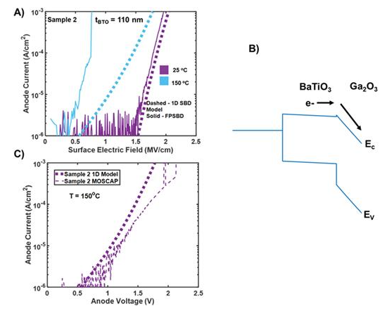
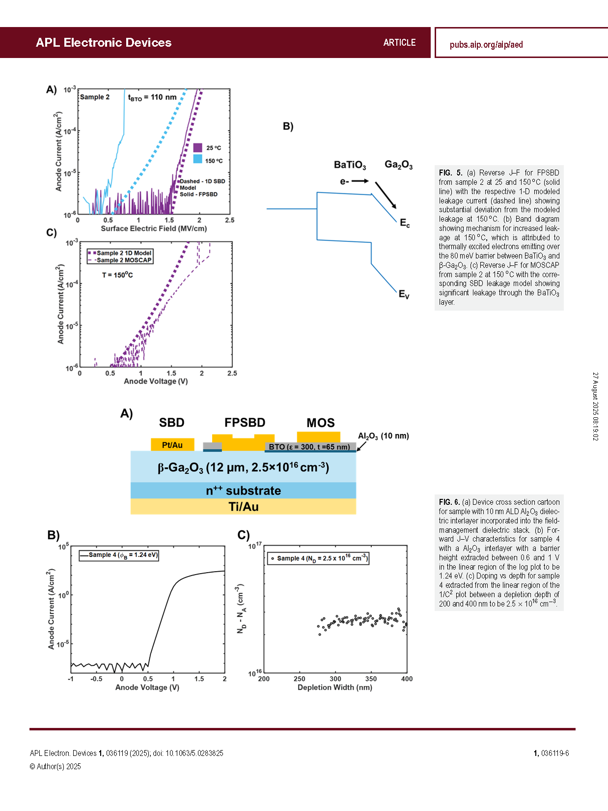
FIG. 5. (a) Reverse J–F for FPSBD from sample 2 at 25 and 150 °C (solid line) with the respective 1-D modeled leakage current (dashed line) showing substantial deviation from the modeled leakage at 150 °C. (b) Band diagram showing mechanism for increased leakage at 150 °C, which is attributed to thermally excited electrons emitting over the 80 meV barrier between BaTiO3 and β-Ga2O3. (c) Reverse J–F for MOSCAP from sample 2 at 150 °C with the corresponding SBD leakage model showing significant leakage through the BaTiO3 layer.
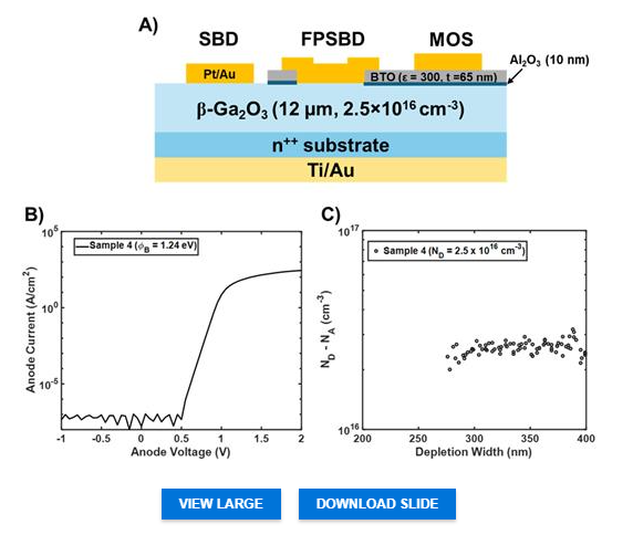
FIG. 6. (a) Device cross section cartoon for sample with 10 nm ALD Al2O3 dielectric interlayer incorporated into the field-management dielectric stack. (b) Forward J–V characteristics for sample 4 with a Al2O3 interlayer with a barrier height extracted between 0.6 and 1 V in the linear region of the log plot to be 1.24 eV. (c) Doping vs depth for sample 4 extracted from the linear region of the 1/C2 plot between a depletion depth of 200 and 400 nm to be 2.5 × 1016 cm−3.
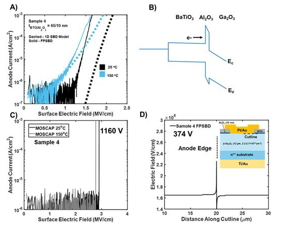
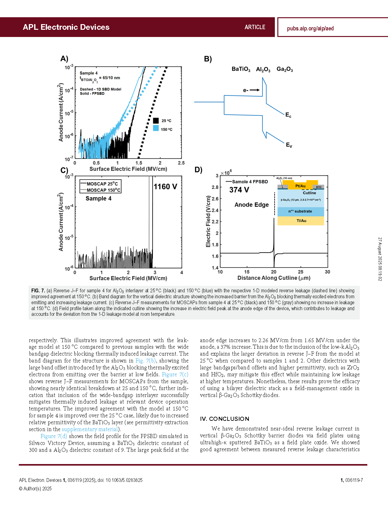
FIG. 7. (a) Reverse J–F for sample 4 for Al2O3 interlayer at 25 °C (black) and 150 °C (blue) with the respective 1-D modeled reverse leakage (dashed line) showing improved agreement at 150 °C. (b) Band diagram for the vertical dielectric structure showing the increased barrier from the Al2O3 blocking thermally excited electrons from emitting and increasing leakage current. (c) Reverse J–F measurements for MOSCAPs from sample 4 at 25 °C (black) and 150 °C (gray) showing no increase in leakage at 150 °C. (d) Field profile taken along the indicated cutline showing the increase in electric field peak at the anode edge of the device, which contributes to leakage and accounts for the deviation from the 1-D leakage model at room temperature.
DOI:
doi.org/10.1063/5.0283825