


Paper Sharing
【Member Papers】Van der Waals β-Ga₂O₃ thin films on polycrystalline diamond substrates
日期:2025-09-02阅读:542
Recently, Professor Zhang Jincheng and Professor Ning Jing from the team of Academician Hao Yue of the Department of Integrated Circuits of Xidian University have made breakthroughs in the field of wide bandgap semiconductor material integration, and the research results are based on "Van der Waals β-Ga₂O₃ thin films" on polycrystalline diamond substrates", which was published online in Nature Communications (DOI: 10.1038/s41467-025-63666-x), and successfully achieved high-quality β-Ga₂O₃ The effective integration of thin films with high thermal conductivity polycrystalline diamond substrates provides a new way to solve the thermal management problems of Gallium Oxide-based electronic devices. Professor Zhang Jincheng is the corresponding author of the paper, and Professor Tranquility and master's student Yang Zhichun are the co-first authors of the paper.
Gallium oxide (β-Ga₂O₃) is regarded as the core material of the next generation of high-power, optoelectronic devices due to its ultra-wide bandgap, high breakdown field strength, and low-cost crystal growth. However, Ga₂O₃'s relatively low thermal conductivity (about 10-30 W/m·K), which is only one-sixth of diamond, poses a huge challenge to high-power semiconductor devices. As the power density of the device increases, the thermal build-up effect rapidly intensifies, leading to performance degradation and limiting the full potential of Ga₂O₃'s high power. Therefore, thermal management has become one of the main technical bottlenecks limiting the development and widespread application of Ga₂O₃-based power devices. The introduction of diamond with high thermal conductivity as a heat dissipation substrate is the most potential thermal management strategy at present. Although monocrystalline diamond substrates have excellent thermal conductivity, their limited wafer size and high preparation costs limit their large-scale application in industry. Therefore, achieving high-quality β-Ga₂O₃ epitaxy on low-cost polycrystalline substrates has become a more feasible technical path, but it faces major challenges such as crystal orientation disorders, multiple interface defects, and thermal stress accumulation.
This study reveals the two-dimensional material-assisted β-Ga₂O₃By introducing graphene as the lattice decoupling layer, the lattice dismatch caused by the crystal orientation disorder of polycrystalline diamond substrate was effectively shielded, and the (-201) orientation β-Ga₂ was successfully achieved with the help of weak interface coupling and the oxygen-lattice co-modulation model. The controllable epitaxy of O₃ films has a breakthrough in elucidating the physical mechanism of the growth of single crystal films on polycrystalline substrates assisted by two-dimensional materials.
In this study, the thermal boundary resistance of the β-Ga₂O₃/diamond interface was measured to be only 2.82m2· K/GW, an order of magnitude lower than the existing technology. The photodetector prepared based on the van der Waals heterostructure exhibits a light-dark current ratio of up to 106 and a response of 210 A/W, confirming its significant advantages in thermal management and optoelectronic performance, providing a new solution to the thermal management problem of Gallium Oxide-based high-performance power electronic devices, realizing the efficient integration of high thermal conductivity substrates and ultra-wide bandgap semiconductors, and promoting the next generation of high power. The development of rate devices is of great significance.
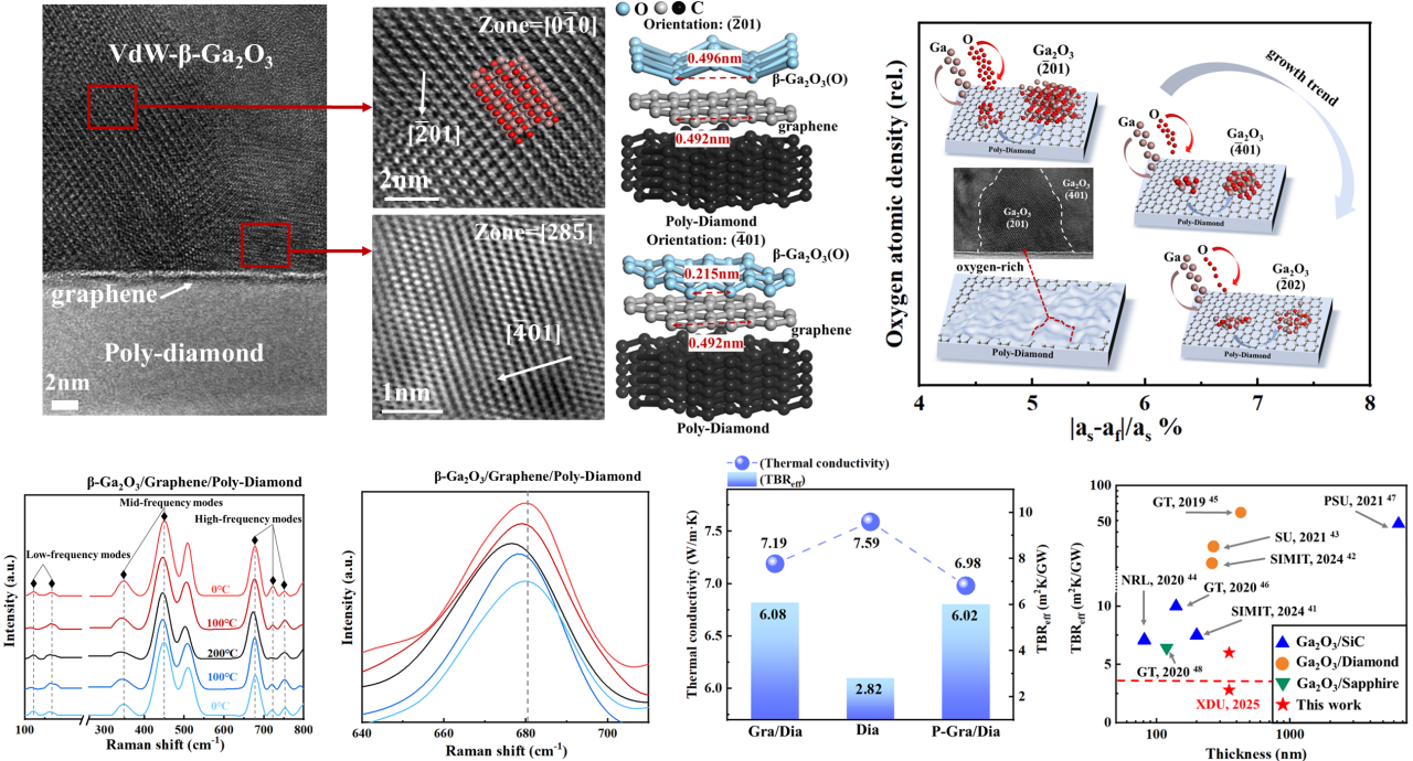
Fig. High thermal conductivity diamond-based gallium oxide epitaxial film and its regulatory model
Link
https://www.nature.com/articles/s41467-025-63666-x#article-info
