


Paper Sharing
【International Papers】Atomic-Scale Investigation of Defect Formation and Phase Transformation in Ir-Deposited Ga₂O₃ Schottky Diodes
日期:2025-09-02阅读:577
Researchers from The Ohio State University have published a dissertation titled "Atomic-Scale Investigation of Defect Formation and Phase Transformation in Ir-Deposited Ga2O3 Schottky Diodes" in Microscopy and Microanalysis.
Main content
Among the different polymorphs of gallium oxide (Ga2O3), monoclinic β-Ga2O3 remains the most thermodynamically stable and is thus the preferred choice for next-generation power electronics. However, its electronic and structural properties can be significantly altered by external stimuli such as metal deposition, ion implantation, and annealing, leading to defect formation, phase transformations and eventually to premature dielectric breakdown. Moreover, in high-power and high-frequency applications, where devices might experience extremely high electric fields, thermal cycling, mechanical stress, and oxidation, which can interact synergistically to accelerate material degradation. Understanding the fundamental atomic-scale mechanisms governing defect formation and phase stability is essential for improving the resilience of β-Ga2O3-based devices in demanding environments.
Recent studies have revealed that point-defect complexes, particularly divacancy-interstitial complexes, play a critical role in governing the electronic properties of β-Ga2O3. Ritter et al. identified Ir-related defects at the Ga2O3 interface can significantly affect the electrical properties of β- Ga2O3. This study aims to employ high-resolution STEM and advanced microanalysis to examine defect formation and phase transformations at the interface of Ir-deposited β-Ga2O3 Schottky diodes.
Preliminary observations from high-resolution STEM imaging on both [010] and [001] suggest atomic structural distortions at the Ir/Ga2O3 interface, indicating possible diffusion of Ir defects through the interface. The pathways of diffusion of Ir defects are observed to change with respect to the sample orientation. Similar studies on Ni/Ga2O3 have shown that metal diffusion can lead to defect accumulation and β to γ phase transformation in some instances. High-angle annular dark field (HAADF) imaging as shown in Fig.1 highlights localized defect clusters appearing as regions of reduced intensity within the Ga2O3 matrix. Previous investigations on ion-implanted β-Ga2O3 have demonstrated that such structural distortions can serve as an initiating site for β- to γ-Ga2O3 transformation. A similar mechanism might be there at the Ir/β-Ga2O3 interface, where interfacial stress and atomic interdiffusion could influence structural modifications to cause the dielectric breakdown.
To further understand the nature of these defects, and variation in their diffusion pathways, several key analyses are planned. Firstly, we would conduct in-depth examination of the obtained images to observe any possible connection among phase transformation, dislocation networks formation and dielectric breakdown. We anticipate different level of atomic diffusion into the matrix and therefore, formation of vacancy complex in different heights from the interface in two distinct directions. Previous reports on Ga2O3 have identified that when the density of such dislocations surpasses a critical threshold, it may cause the stabilization of a metastable γ-Ga2O3 phase. We intend to observe if there any such transformations occurring in Ir/β-Ga2O3 sample which could have caused the breakdown of the diode.
By linking atomic-scale structural changes to dielectric breakdown mechanisms, this work aims to provide critical insights into the degradation of ultra-wide-bandgap semiconductors under extreme operating conditions, which will contribute to the advancements of robust materials for power and energy-related applications.
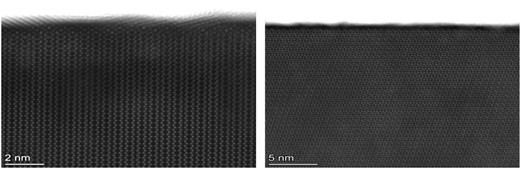
Fig. 1. HAADF STEM images for the reference Ir deposited β-Ga2O3 sample (a) along [010] direction and (b) along [001] direction.
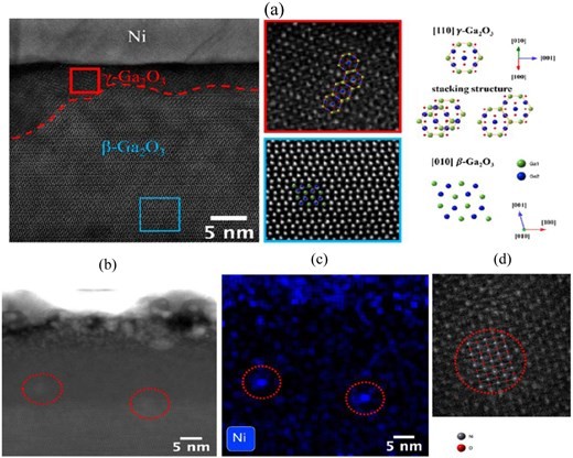
Fig. 2. (a) HAADF-STEM image of the β-Ga2O3/Ni diode interface in as-deposited condition. The red and blue rectangles indicate magnified regions of the γ-phase and β-phase Ga2O3, respectively. In the red rectangle, the atomic structure follows the [110] γ-Ga2O3 stacking sequence. In the blue rectangle region, crystal structure corresponds to [010] β-Ga2O3. Post-breakdown characterization of a β-Ga2O3/Ni diode following air exposure, (b) HAADF-STEM image showing NiO clusters (highlighted by red circles). (c) EDX elemental mapping confirming the presence of NiO. (d) A magnified view of the NiO clusters, revealing their structural characteristics.
DOI:
doi.org/10.1093/mam/ozaf048.784
