Paper Sharing
【International Papers】p-type layer formation study for Ga₂O₃ by employing Ni ion implantation with two-step oxygen plasma and thermal annealing
日期:2025-09-02阅读:681
Researchers from the Nagoya University have published a dissertation titled "p-type layer formation study for Ga2O3 by employing Ni ion implantation with two-step oxygen plasma and thermal annealing" in Journal of Applied Physics.
Background
Ga2O3 is well known to be a promising material for next-generation efficient power devices. Baliga's figure of merit (BFOM) for unipolar devices increases in the order Si, SiC, GaN, Ga2O3, and diamond. In compound semiconductors, crystal quality and practical acceptor-doped p-type and donor-doped n-type layer formation technologies are keys to expanding the diversity and scalability of devices. In practice, SiC-based Schottky barrier diodes are replacing Si devices in inverter applications. However, high production costs due to SiC substrates being deposited by physical vapor deposition (PVD) and high device processing temperatures are barriers to increasing their market scale. SiC also faces another difficulty in that it tends to degrade when used in bipolar pn junction devices. Ga2O3 is a potential alternative because it is less expensive to produce than SiC as a result of its compatibility with melt-growth methods such as the film-fed growth8 or Czochralski method. Schottky barrier diodes based on Ga2O3 are under development; however, practical bipolar pn diodes have not yet been achieved.
Many candidates for p-type dopants have been studied. Among them, p-type NiO as a hetero structural deposition layer on Ga2O3 substrates was proposed and tested. The sputtering method, pulsed laser deposition method, polyol reduction method, and Ni alloying method were applied. Researchers found that these layers are feasible for electric-field relaxation or hole injection. In the case of sputtered NiO layer films, however, a highly durable and reliable p-layer with molecular-level homogeneous contact with a Ga2O3 substrate is difficult to achieve. This problem is similar to that encountered with SiO2 layers on Si devices. It is well known that only a thermal oxide SiO2 layer, not a sputtered SiOx layer, is applicable as the metal oxide–semiconductor (MOS) layer or the essential passivation layer for practical Si power devices because of its crystalline nature. Unlike thermally oxidized SiO2 films, which have stable impurity connection layers, amorphous SiOx and sputtered impurity layers are not able to provide practical and reliable power devices. The generation of a stable junction while maintaining crystallinity between the Si substrate and the oxidized SiO2 layer requires molecular-level interdiffusion between each layer. Therefore, in the present study, we refer to the stable thermal oxidation of Si substrates. The aim of this study is to fabricate a practical p-type role layer for Ga2O3 devices applicable to any process and design, such as hole injection and junction stabilization of Ga2O3 devices.
Abstract
We demonstrated stable local or planar p-type layer formation for Ga2O3. Our concept is to use NiO as the dopant. The process comprises as follows: 58Ni ion implantation into Ga2O3 substrates, followed by activation and crystallinity improvement of implanted 58Ni, and formation of NiO doped layers by applying low-temperature O-radical-based plasma annealing (O-PA) and O2 rapid thermal annealing (O2-RTA). Basic experiments were conducted to clarify the validity of this concept. Results showed that O-PA was more effective than O2-RTA in repairing damage induced by 58Ni implantation. Typical layer evaluation results, including forward and reverse directional electrical characteristics of Ga2O3 diode structures [“NiO doped:” Ni/Ga2O3:NiO(p)/Ga2O3:Sn (n)/Ti, and “Ni/Schottky:” Ni/Ga2O3:Sn (n)/Ti] fabricated using Ga2O3 substrates, are shown. The NiO doped diodes were fabricated using the highest Ni implantation concentration of 1020 cm−3, followed by O-PA and O2-RTA. The NiO doped diodes annealed using two-step annealing, low-temperature O-PA (300 °C, 1 h) and O2-RTA (950 °C, 1 h), showed distinct bipolar rectification characteristics with a forward conduction capability more than twice that of the Ni/Schottky diode. The NiO doped diode surface was evaluated by electron diffraction (ED) analysis. The diffraction pattern for the NiO doped area was that of Ga2O3 but differed somewhat from the pattern for the Ga2O3 substrate. The NiO doping process is considered to generate acceptors in the doped area. We expect our proposed concept to lead to bipolar Ga2O3 devices and other bipolar compound semiconductors with practical acceptor layers.
Conclusion
From this study, we obtained the following results. The implantation of Ni at higher concentrations (e.g., 1020 to 1018 cm−3) led to a higher resistivity of the implanted area. In the beginning, we intended to make the Ni-implanted area low resistive. In the case of Si, we could attain a p-type layer with a low acceptor energy level and low resistance by p-type impurity ion implantation and thermal annealing. The layer in this study was confirmed to be a single-crystal layer with the role and function of p-type conductivity. However, because a low resistance layer was not achieved, we speculate that the layer is characterized by a deep acceptor energy level. Nevertheless, we continued our investigation under the consideration that the annealing condition that reduces the implanted-layer resistivity can produce a crystallized p-type layer in Ga2O3.
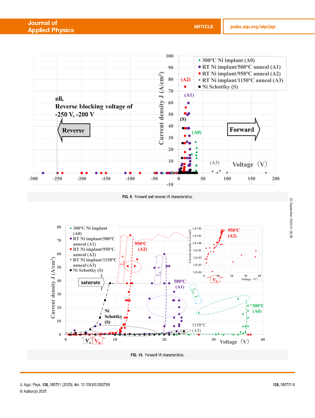
Notably, implantation of 58Ni at a concentration 1020 cm−3 with two-step annealing, O-PA (300 °C, 1 h) and O2-RTA at 950 °C for 10 min led to a device with a forward-current density of 74 A/cm2 (60 Hz), which is more than twice as large as the maximum value for a Ni/Schottky diode fabricated on the same substrate. The feature of this NiO doped diode, which showed an initial voltage (V*) of ∼5 V, comparable to the pn built-in potential in Ga2O3 (4.8 V), was detected under this forward-current conduction analysis.
From these results, the first O-PA conditions of 300 °C and 1 h are considered to activate the ion-implanted Ni into Ni oxide via low-temperature annealing, where Ga2O3 can be crystallized without decomposing.46 In contrast, the poor conduction characteristics of NiO doped diode A4 annealed at 700 °C (O-PA) were attributed to crystal decomposition. In contrast, the poor conduction characteristics of NiO doped diode A4 annealed at 700 °C (O-PA) were attributed to crystal decomposition. The reduction in crystal defects and the formation and activation of bonds thought to be Ni–O–Ga are considered to be determined by the balance with the thermal decomposition of Ga2O3. In addition, a second O2 thermal O2-RTA (500–1150 °C, 10 min) is thought to activate carriers in the Ga2O3:NiO thin layer by the O-PA treatment and to increase the carrier density, similar to the effects of the conventional annealing method. These 10 min annealing processes are sufficiently short to prevent the decomposition of Ga2O3. SIMS, SR, TEM, and ED analyses clarified that the proposed layer is a crystal layer and composed of NiO in a Ga2O3 substrate, with a thickness of 0.1 μm. This anode surface thin crystal layer is considered to inject holes into the Ga2O3 substrate.
We conclude that Ni-ion implantation and two successive annealing procedures enable the fabrication of a practical p-type layer with NiO impurities, expected to be Ga2O3:NiO in Ga2O3. The advantage of this method is its use of common ion implantation and annealing methods, which are applicable to various devices. We believe that our proposed method is a bipolar device fabrication method that will be widely applied to compound semiconductors.
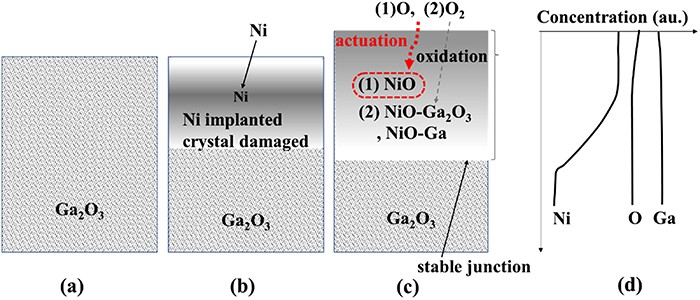
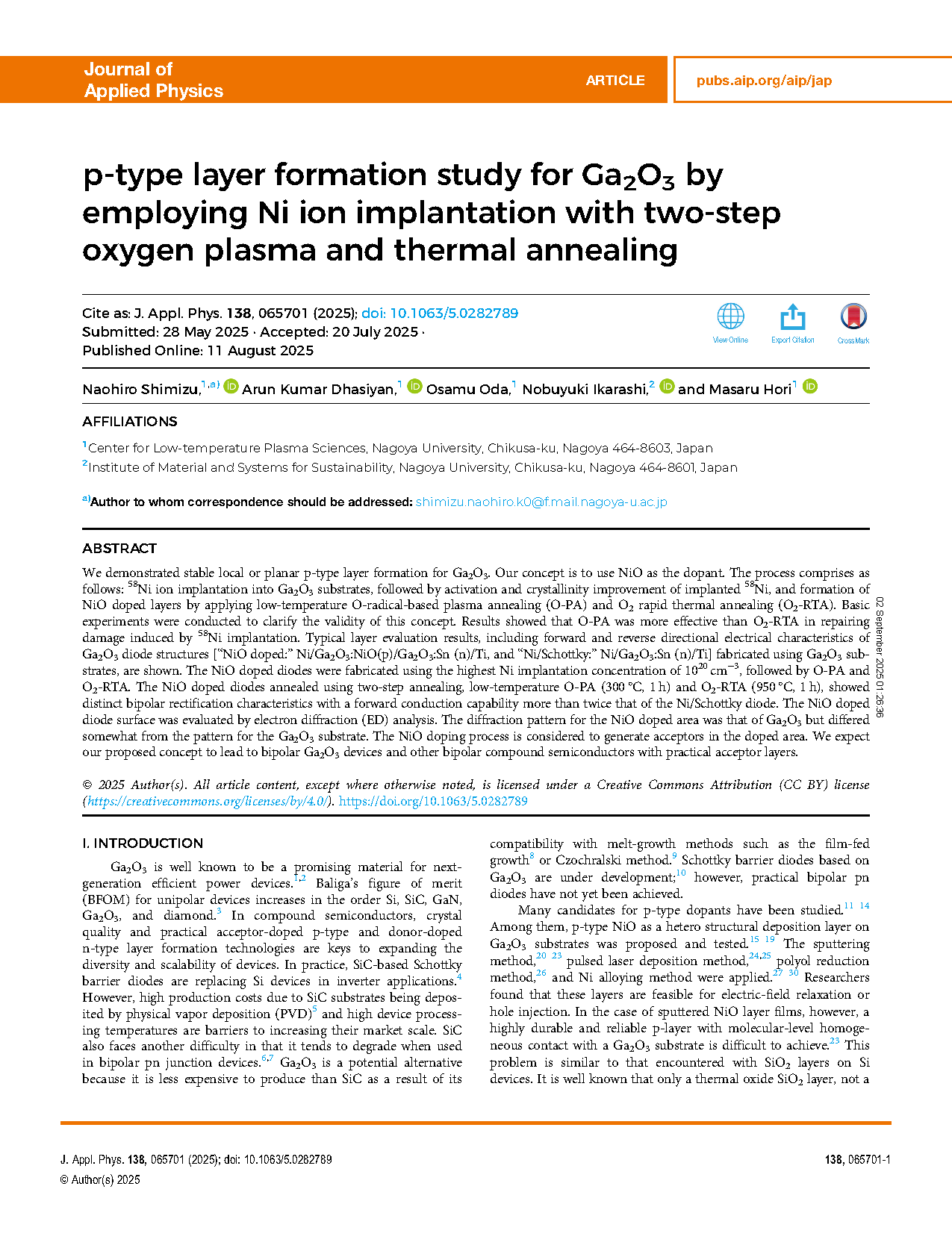
FIG.1 Acceptor doping concept for Ga2O3. (a) Ga2O3 substrate. (b) Ni implantation. (c) (1) O actuation, (2) O2 oxidation and anneal for crystallization. (d) Material concentration distributions.
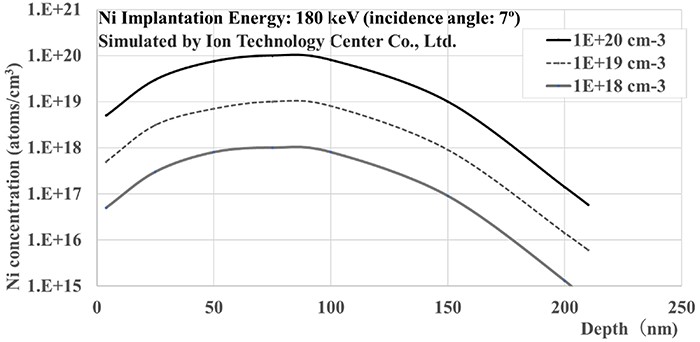
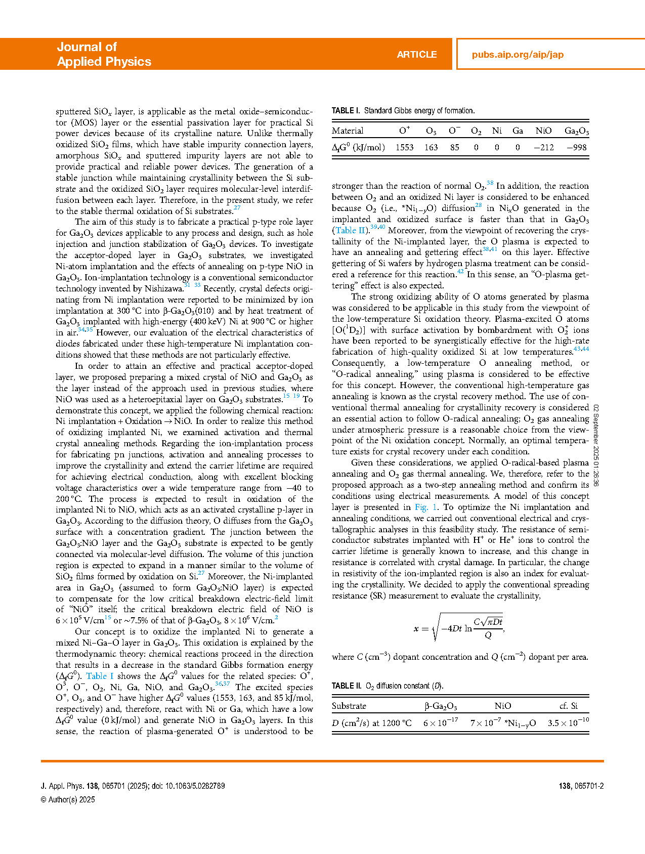
FIG.2 Implanted Ni depth and concentration profile in the Ga2O3 substrate.
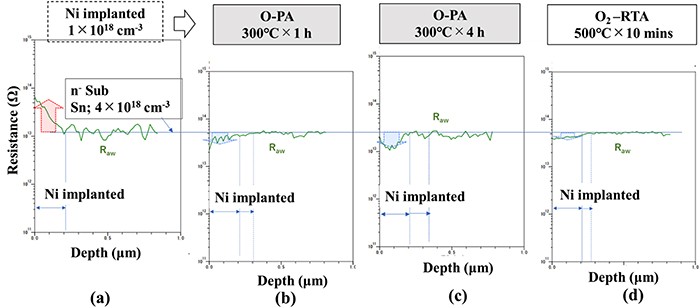
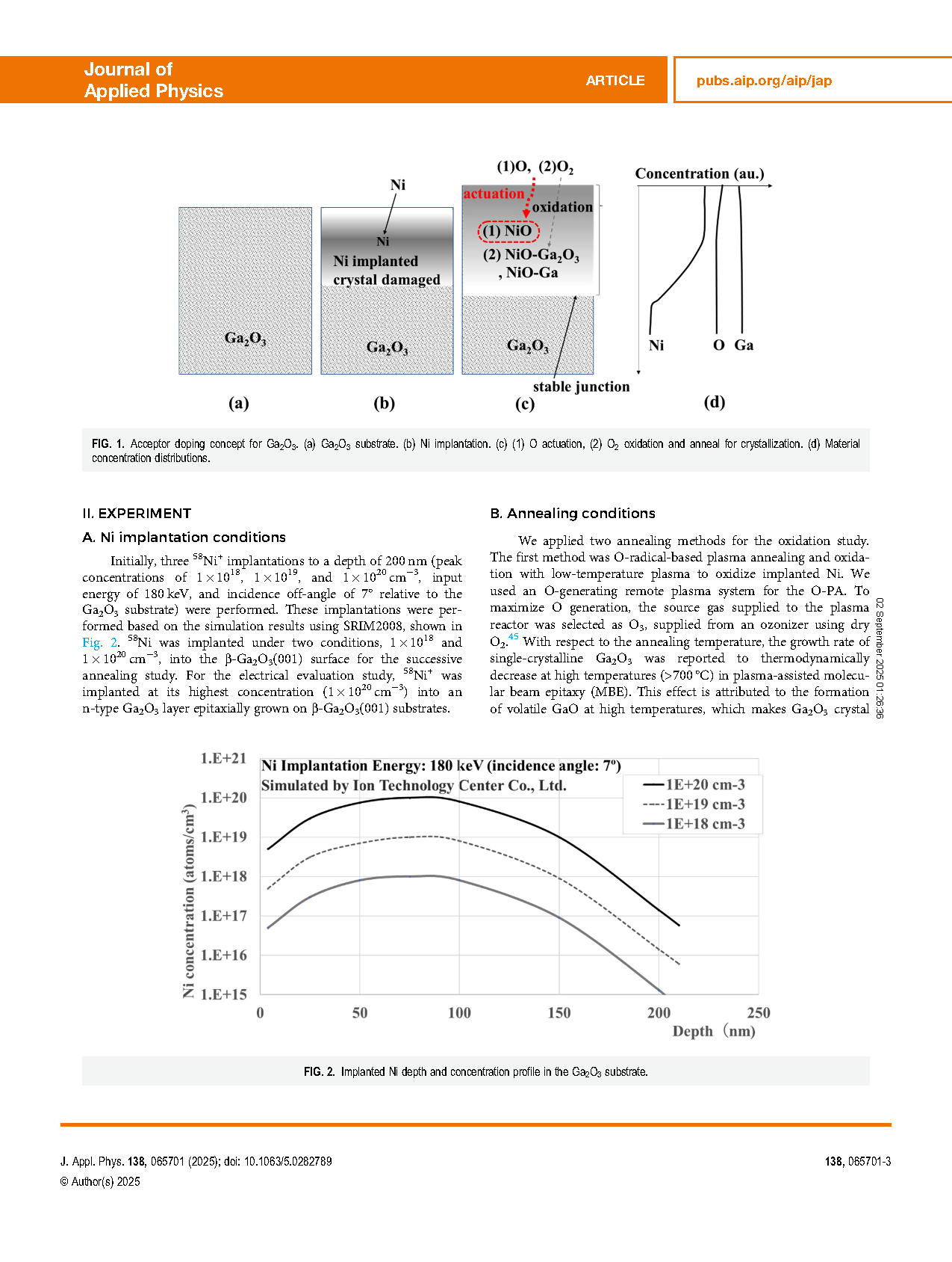
FIG.3 SR analysis of Ni 1 × 1018 cm−3 implanted β-Ga2O3 substrate and of annealed substrates (a) as Ni implanted. (b) After O-PA (300 °C × 1 h). (c) After O-PA (300 °C × 4 h). (d) After O2-RTA (500 °C × 10 min).
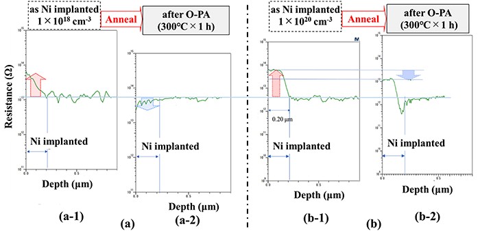
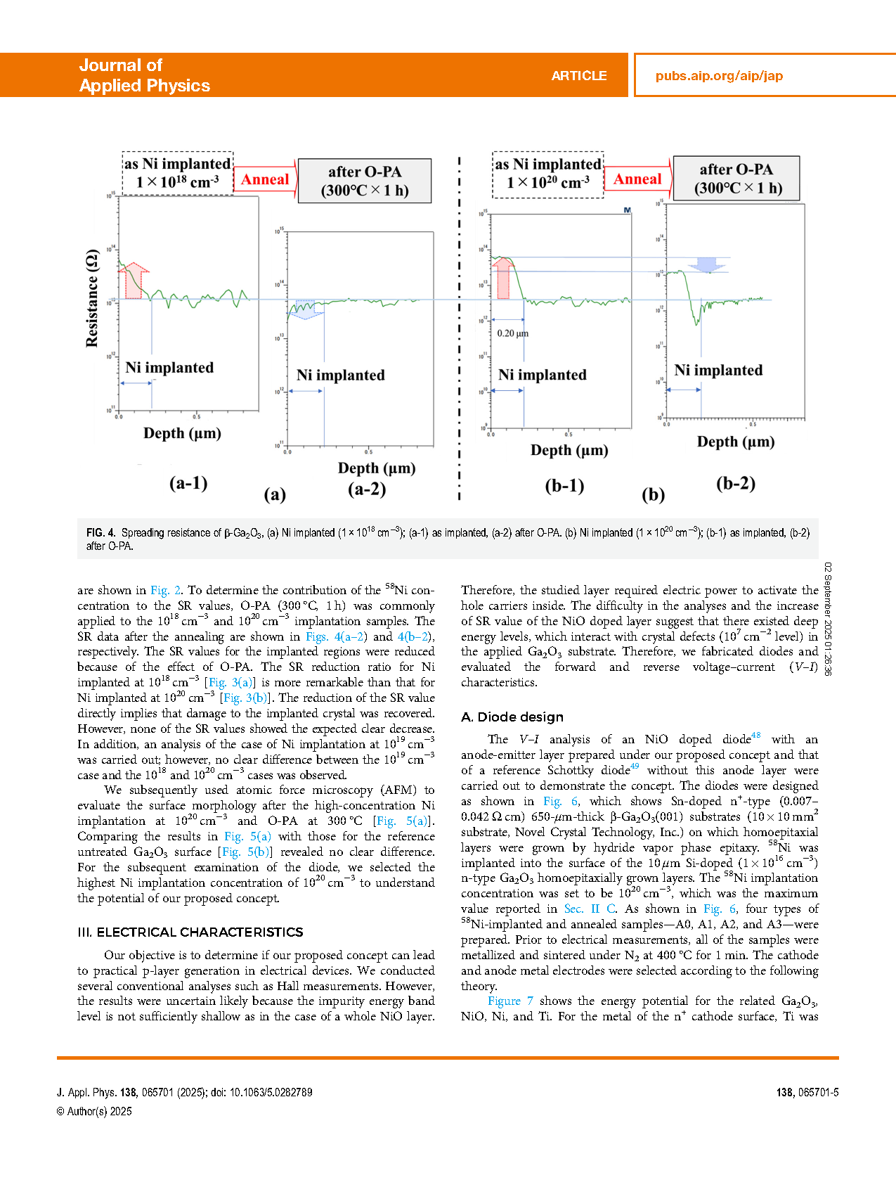
FIG.4 Spreading resistance of β-Ga2O3, (a) Ni implanted (1 × 1018 cm−3); (a-1) as implanted, (a-2) after O-PA. (b) Ni implanted (1 × 1020 cm−3); (b-1) as implanted, (b-2) after O-PA.
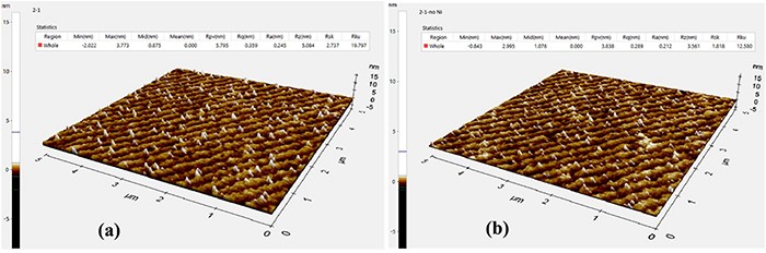
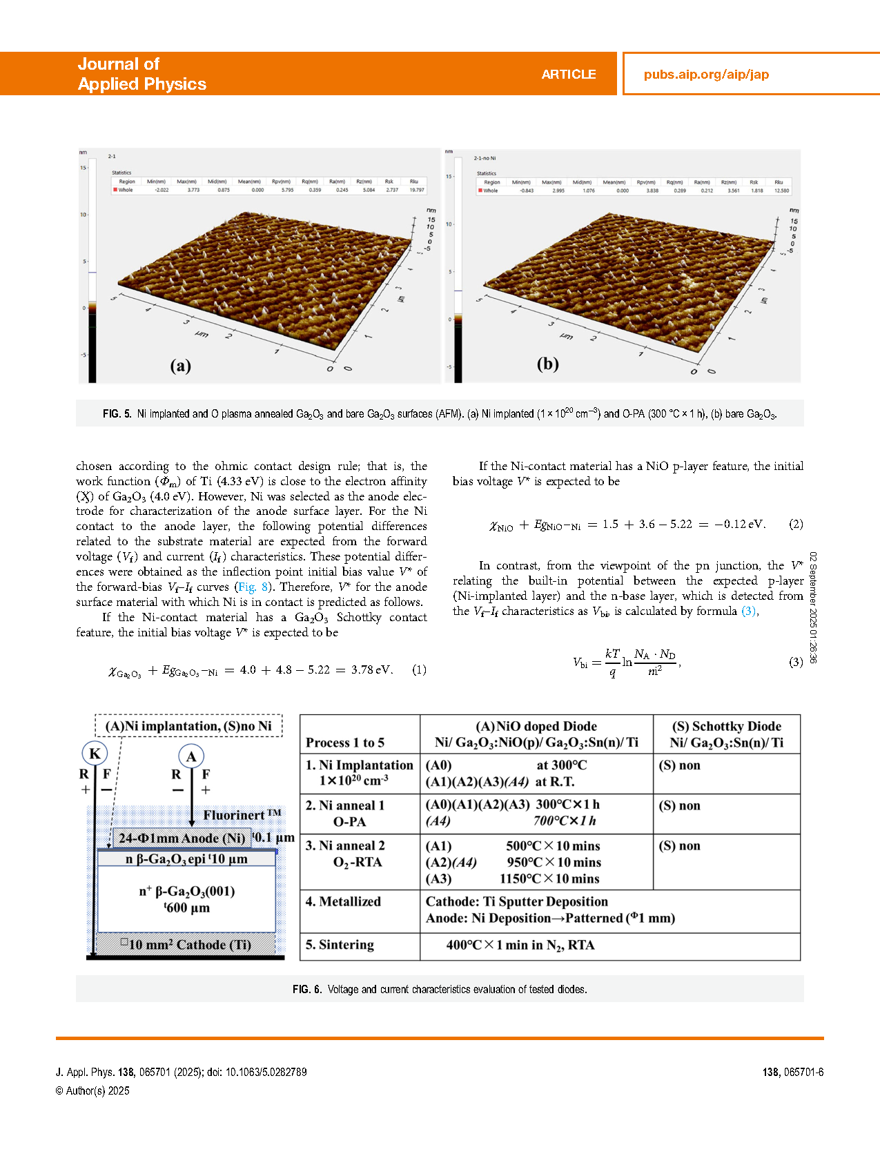
FIG.5 Ni implanted and O plasma annealed Ga2O3 and bare Ga2O3 surfaces (AFM). (a) Ni implanted (1 × 1020 cm−3) and O-PA (300 °C × 1 h), (b) bare Ga2O3.
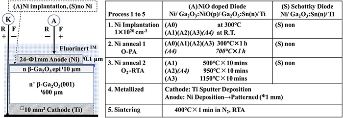
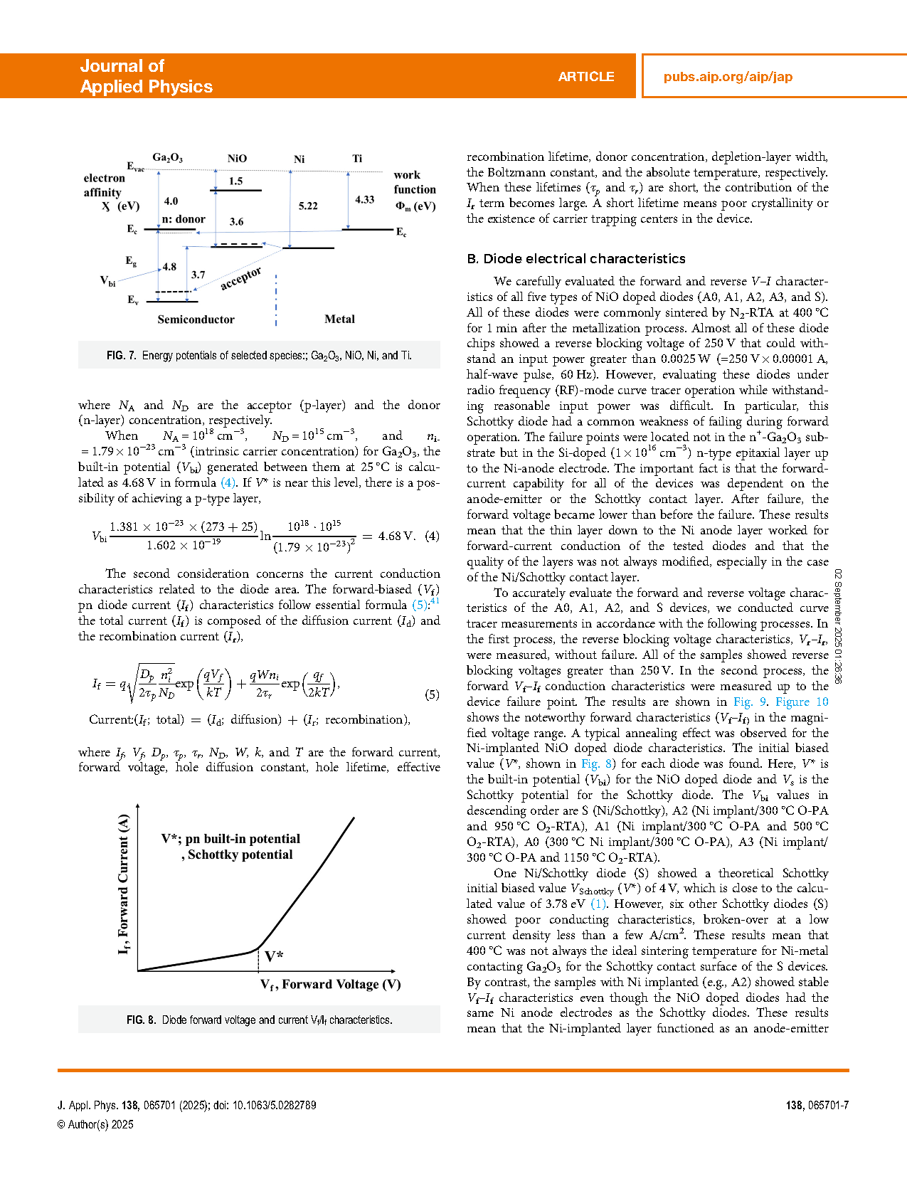
FIG.6 Voltage and current characteristics evaluation of tested diodes.
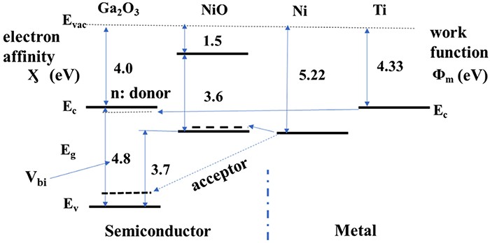
FIG.7 Energy potentials of selected species:; Ga2O3, NiO, Ni, and Ti.
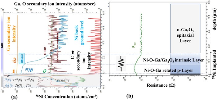
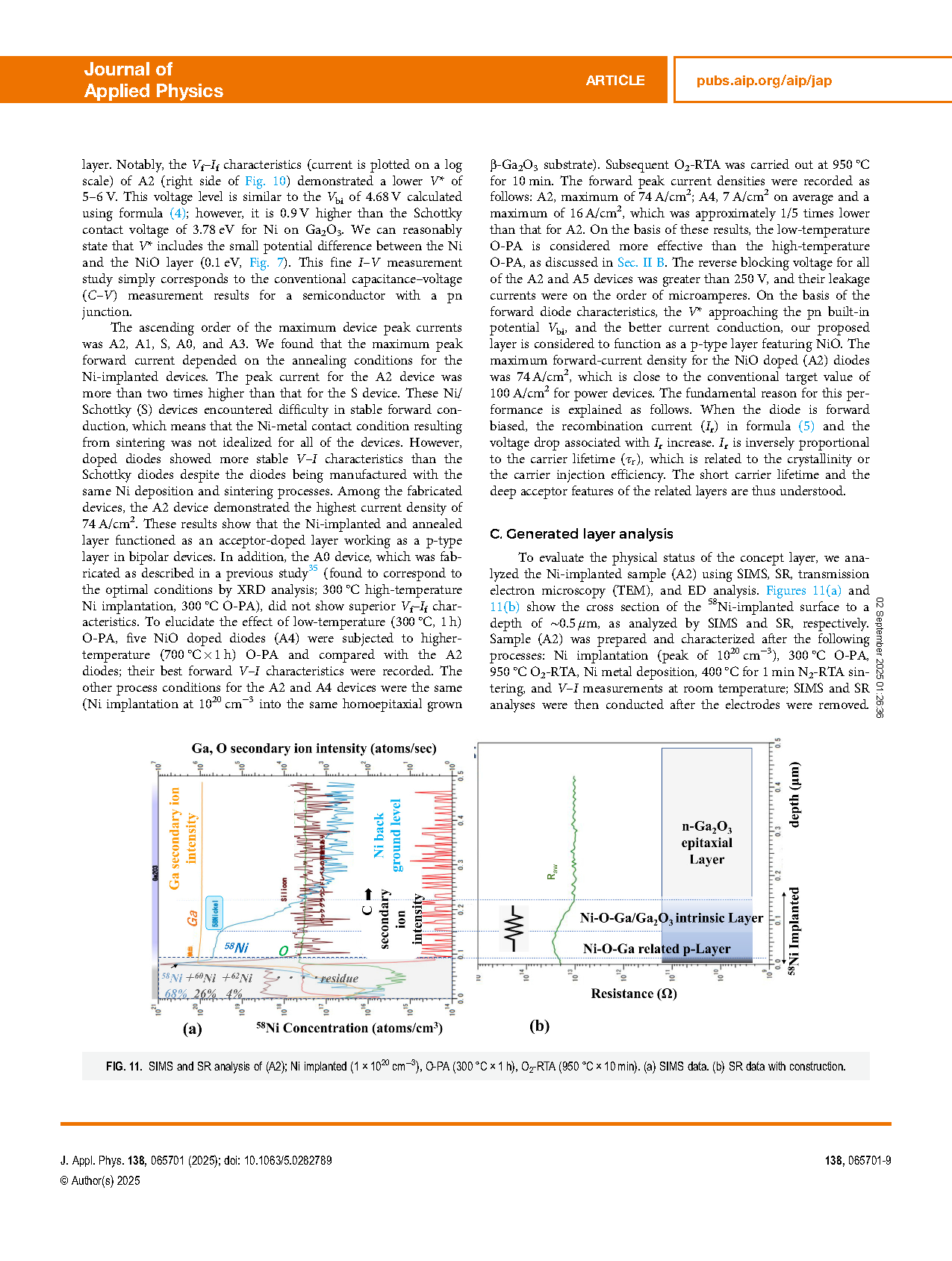
FIG.8 SIMS and SR analysis of (A2); Ni implanted (1 × 1020 cm−3), O-PA (300 °C × 1 h), O2-RTA (950 °C × 10 min). (a) SIMS data. (b) SR data with construction.
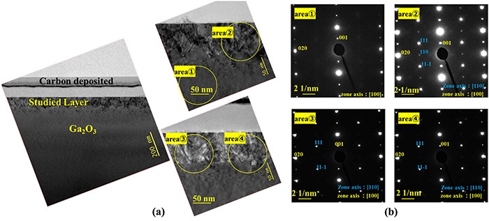
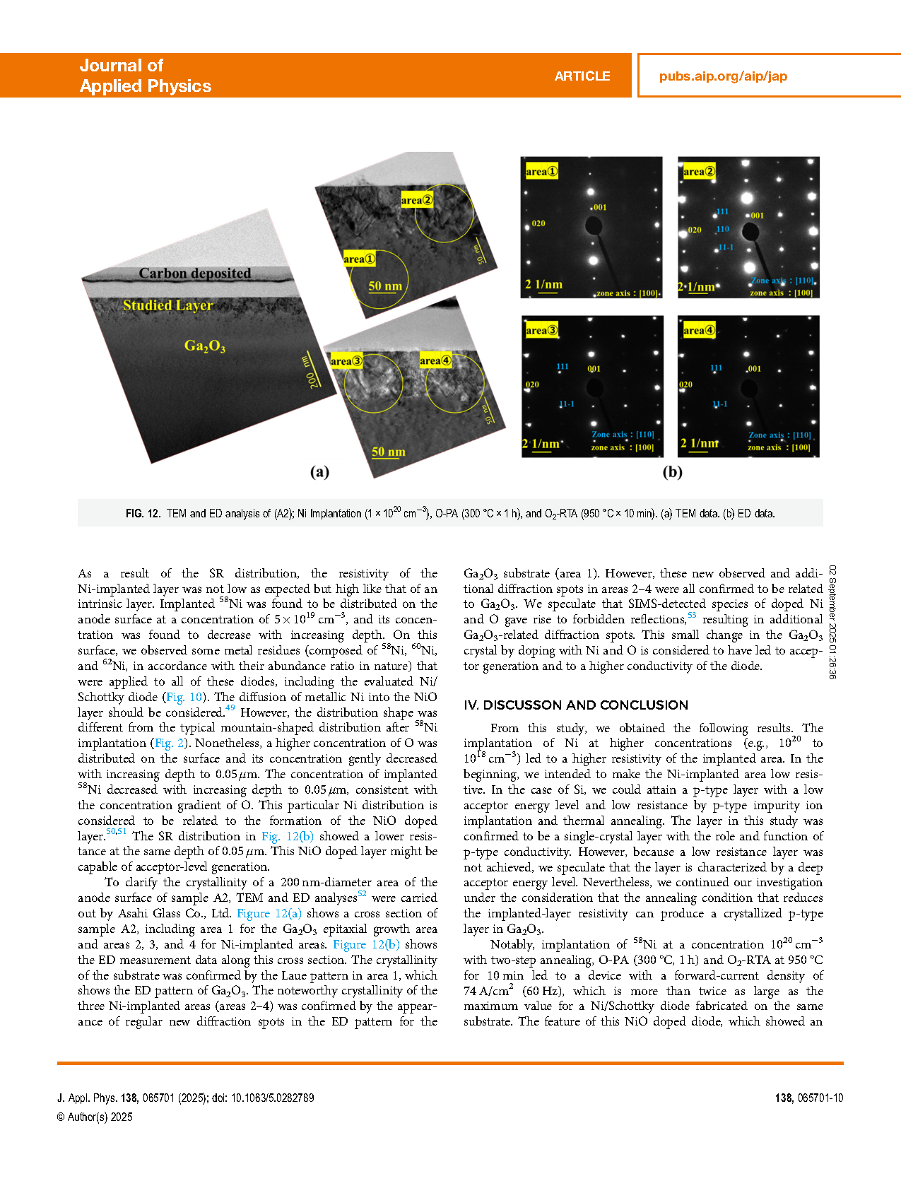
FIG.9 TEM and ED analysis of (A2); Ni Implantation (1 × 1020 cm−3), O-PA (300 °C × 1 h), and O2-RTA (950 °C × 10 min). (a) TEM data. (b) ED data.
DOI:
doi.org/10.1063/5.0282789