Paper Sharing
【Domestic Papers】In situ nitrogen doping of β-Ga₂O₃ during MOCVD homoepitaxy: A theoretical and experimental study
日期:2025-09-04阅读:608
Researchers from the Fuzhou University and the Hangzhou Institute of Optics and Fine Mechanics have published a dissertation titled "In situ nitrogen doping of β-Ga2O3 during MOCVD homoepitaxy: A theoretical and experimental study" in Applied Physics Letters.
Project Support
This work was financially supported by the National Natural Science Foundation of China (Grant No. 62204270), the Major Science and Technology Special Project of Fujian Province (Grant No. 2022HZ027006), the Fujian Provincial Natural Science Foundation General Program (Grant No. 2024J01251), the Fujian Provincial Science and Technology Program Project (Grant No. 2022I0006), and the Major Science and Technology Special Project of Quanzhou Municipality (Grant No. 2022GZ7). The authors also thank Fujia Co. Ltd. for help in the growth of epitaxial films.
Background
The development of Ga2O3-based high-voltage power devices is hindered by the absence of a reliable p-type epilayer slow progress in high-quality current-blocking layers and high-performance drift layers, and most critically, the lack of precise control over acceptor dopant concentrations. In the preparation of high-quality β-Ga2O3 homoepilayers using metalorganic chemical vapor deposition (MOCVD), N2O serves as an effective oxygen (O) source that suppresses pre-reactions. However, nitrogen (N) from N2O acts as an acceptor dopant and exhibits significant self-compensation effects with unintentional donor impurities in β-Ga2O3. Consequently, the electrical characteristics of β-Ga2O3 homoepilayers undergo substantial alterations with variations in N doping concentration, fundamentally changing their conductive properties.
Abstract
The precise control of acceptor doping concentrations in epilayers is critical for fabricating key β-Ga2O3-based power electronic structures, including current-blocking layers, p-type epilayers, and drift layers. Unintentional nitrogen (N) compensating dopants introduced by N2O (a common oxygen precursor) during β-Ga2O3 metalorganic chemical vapor deposition growth significantly affects electrical properties. This study demonstrates that N concentration in epilayers is largely determined by growth temperature and surface adsorption efficiency. As the epitaxial temperature increases, the N doping concentration in the epilayer decreases. When the epitaxial temperature exceeds 1000 °C, the efficiency of N adsorption on β-Ga2O3 surfaces is influenced by both epitaxial parameters and substrate orientation. Modifying epitaxial parameters, especially by increasing chamber pressure, enhances the N concentration in β-Ga2O3 epilayers. Stronger N adsorption occurs on the (100)-plane compared to the (001)-plane epilayer; however, the (001)-plane epilayer allows better N concentration tuning through adjustments in parameters. First-principles calculations indicate that such observed differences in adsorption efficiency are attributable to variations in adsorption energies specific to each plane, coupled with competitive interactions between nitrogen (N) and oxygen (O) atoms during surface reactions. This study offers fundamental insights that advance the engineering of β-Ga2O3 homoepilayers for power electronics applications.
Conclusion
This study elucidates the orientation-dependent N doping behavior in β-Ga2O3 homoepilayers grown on (100)- and (001)-planes via MOCVD, combined with first-principles calculations. Key findings reveal that N-incorporation efficiency is dominantly controlled by epitaxial temperature, surface adsorption dynamics, and crystallographic orientation above 1000 °C. Guided by modeling, we establish a competitive N/O adsorption framework accounting for epitaxial environment effects. The observed plane-dependent doping heterogeneity stems from the interplay between chemical potential and adsorption energy anisotropy: N exhibits stronger adsorption stability on the (100)-plane, enabling higher incorporation at elevated temperatures, whereas weaker adsorption on the (001)-plane enhances sensitivity to parameters like chamber pressure. This work provides (1) a crystallographic-orientation mechanism for dopant control, (2) an experimental–theoretical model for competitive adsorption, and (3) pressure-modulation strategies for precision doping in anisotropic semiconductors.
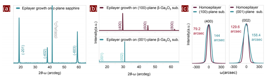
FIG. 1. (a) XRD 2θ-ω scan of the β-Ga2O3 heteroepilayer. (b) XRD 2θ-ω scans of β-Ga2O3 homoepilayers and (c) XRCs of β-Ga2O3 homoepilayer and substrate for the (100)- and (001)-planes, respectively.
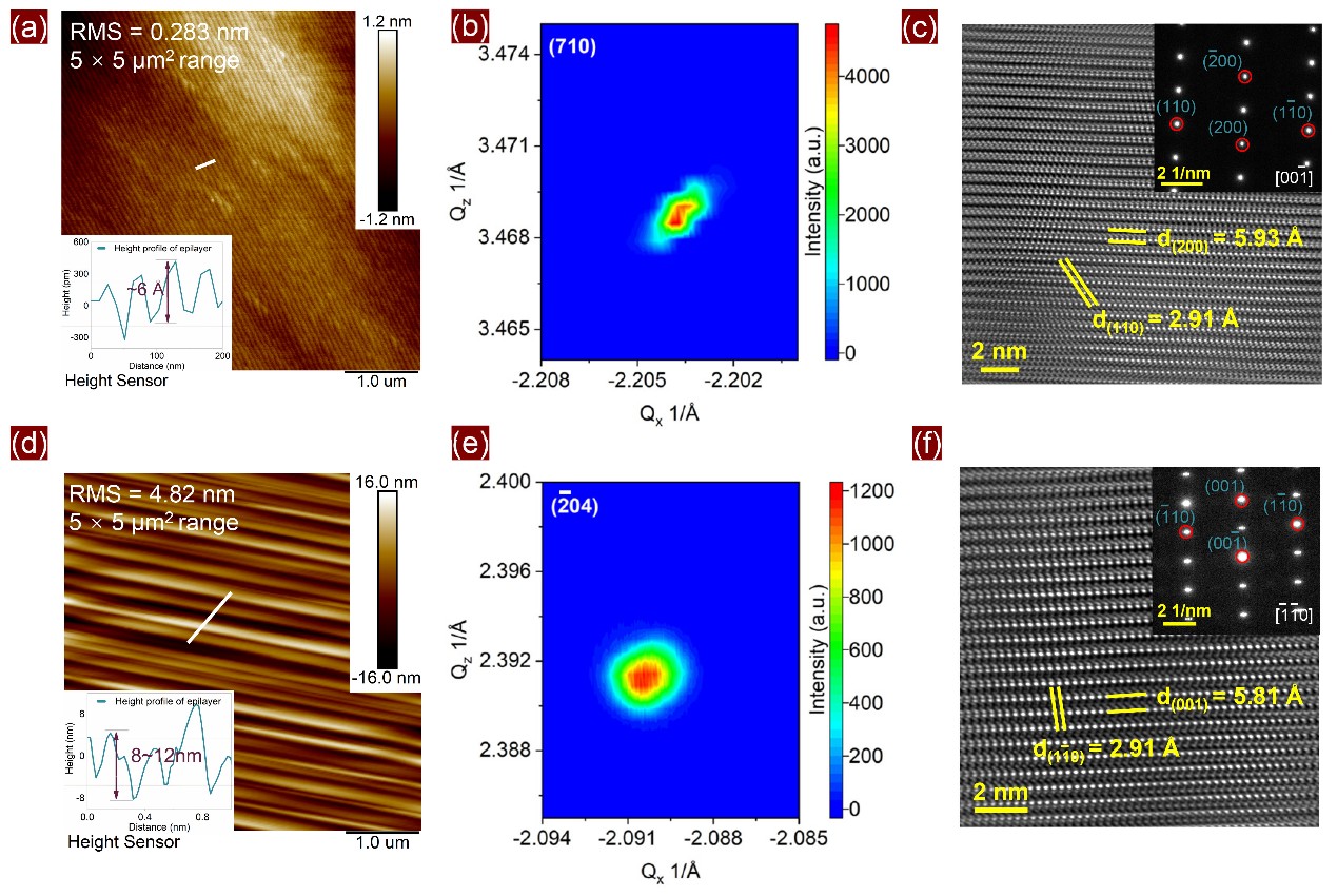
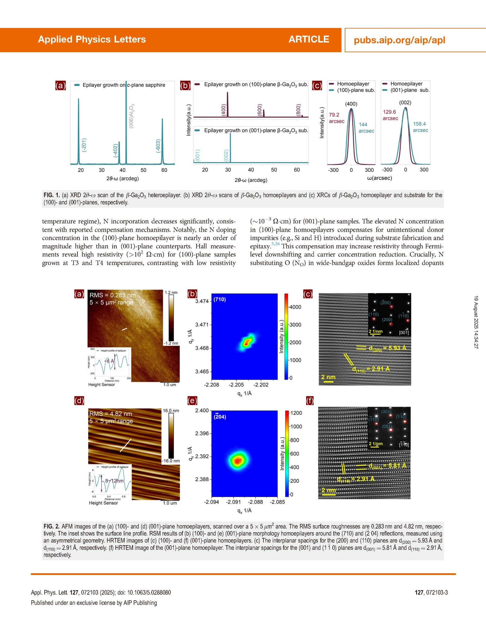
FIG. 2. AFM images of the (a) (100)- and (d) (001)-plane homoepilayers, scanned over a 5×5 μm2 area. The RMS surface roughnesses are 0.283 nm and 4.82 nm, respectively. The inset shows the surface line profile. RSM results of (b) (100)- and (e) (001)-plane morphology homoepilayers around the (710) and (-204) reflections, measured using an asymmetrical geometry. HRTEM images of (c) (100)- and (f) (001)-plane homoepilayers. (c) The interplanar spacings for the (200) and (110) planes are d(200) = 5.93 Å and d(110) = 2.91 Å, respectively. (f) HRTEM image of the (001)-plane homoepilayer. The interplanar spacings for the (001) and (10) planes are d(001) = 5.81 Å and d (110) = 2.91 Å, respectively.
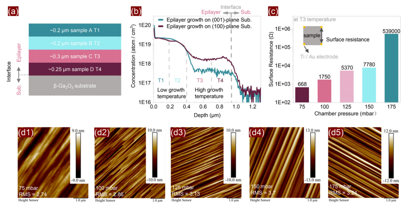
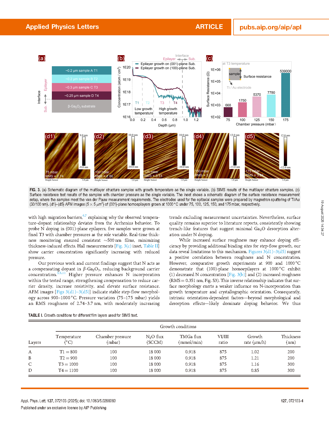
FIG. 3. (a) Schematic diagram of the multilayer structure samples with growth temperature as the single variable. (b) SIMS results of the multilayer structure samples. (c) Surface resistance test results of the samples with chamber pressure as the single variable. The inset shows a schematic diagram of the surface resistance measurement setup, where the samples meet the van der Pauw measurement requirements. The electrodes used for the epitaxial samples were prepared by magnetron sputtering of Ti/Au (30/100 nm). (d1)–(d5) AFM images (5 × 5 μm2 ) of (001)-plane homoepilayers grown at 1000 °C under 75, 100, 125, 150, and 175 mbar, respectively.
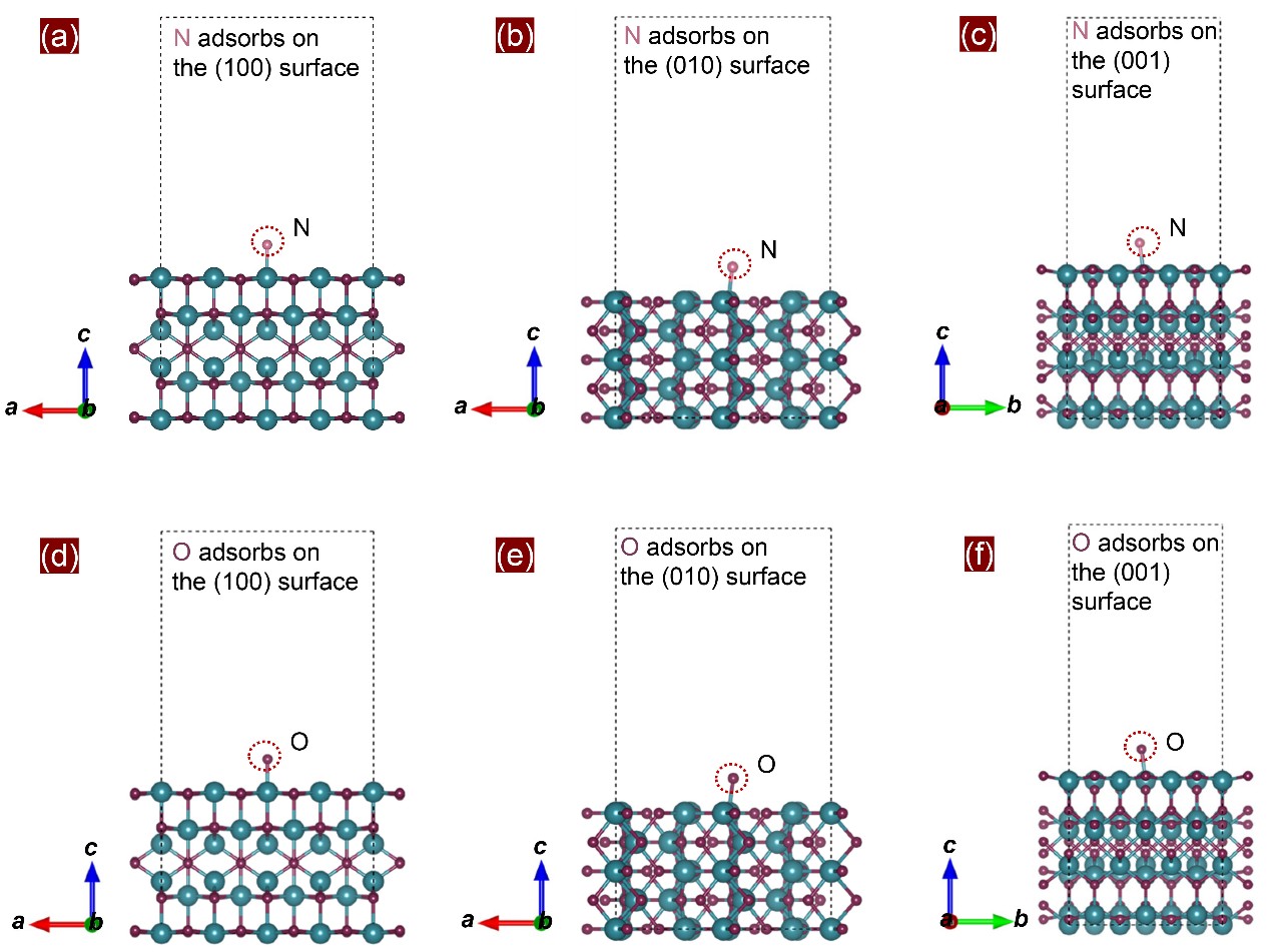
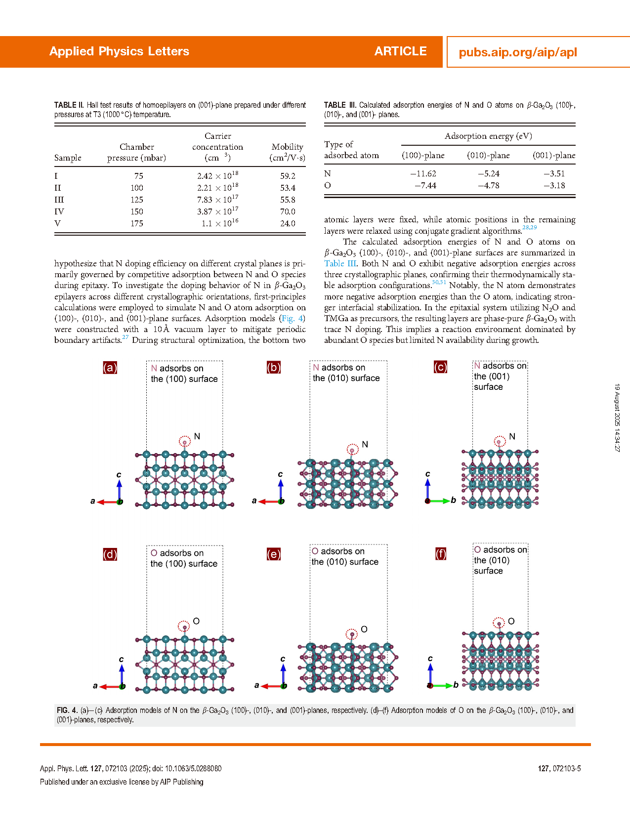
FIG. 4. (a)(c) Adsorption models of N on the β-Ga2O3 (100)-, (010)-, and (001)-planes, respectively. (d)–(f) Adsorption models of O on the β-Ga2O3 (100)-, (010)-, and (001)-planes, respectively.
DOI:
doi.org/10.1063/5.0288080