


Paper Sharing
【Member Papers】High-sensitivity and fast-response solar-blind photodetectors via band offset engineering for motion tracking
日期:2025-09-04阅读:746
Professor Xu Haiyang of Northeast Normal University Professor Ma Jiangang et al. published a paper titled " High-sensitivity and fast-response solar-blind photodetectors via band offset engineering for motion tracking” in Nature Communications.
This study presents A self-powered solar blind photodetector based on a Ga₂O₃/AlN/AlGaN:Si heterostructure, which achieves high responsivity (0.73 A/W) and fast response time (56 μs) through band bending induced by polarization fields. This high-performance photodetector enables 256×256 resolution solar blind single-pixel imaging, which can be used for static fingerprinting and moving target imaging. The proposed band shift engineering strategy opens up new avenues for the development of solar-blind photodetectors and imaging techniques.
Background
Solar-blind photodetection and imaging systems leverage minimal background interference for diverse military and civilian uses—such as secure communications, missile guidance, flame sensing, corona discharge observation. Current systems predominantly employ silicon-based charge-coupled devices (CCDs), complementary metal-oxide-semiconductor (CMOS) sensors, and photomultiplier tubes (PMTs). However, CCDs and CMOS sensors necessitate additional filters to block visible and infrared light, increasing system complexity and weight. PMTs, in contrast, are bulky and require high operating voltages. Ultrawide-bandgap semiconductor focal plane arrays offer a compact alternative for solar-blind imaging, but face challenges related to complex integration process. Recently, several groups have recently reported solar-blind imaging using single ultrawide-bandgap semiconductor photodetector with two-dimensional scanning. Nevertheless, the pixel-by-pixel scanning process remains too slow for real-time imaging. In contrast, the single-pixel imaging technique leverages structured light modulation to capture spatial scene details, utilizing only one photodetector to record the modulated light intensity. This approach offers the benefits of rapid image capture and has recently been demonstrated in the visible and X-ray spectra, positioning it as a promising technology for solar-blind imaging applications.
Abstract
Single-pixel imaging is emerging as a promising alternative to traditional focal plane array technologies, offering advantages in compactness and cost-effectiveness. However, the lack of solar-blind photodetectors combining fast-response and high-sensitivity has constrained their application in the deep ultraviolet spectrum. This work introduces a self-powered solar-blind photodetector based on a heterostructure comprising a Ga2O3 photosensitive layer, an AlN barrier layer, and an N-polar AlGaN:Si contact layer. The polarization field within the AlN layer induces band bending, creating potential wells that confine photogenerated holes and thereby generate photocurrent gain. Consequently, the Ga2O3/AlN/AlGaN:Si solar-blind photodetector achieves a high responsivity of 0.73 A W‒1 and a rapid decay time of 56 µs. This performance enables 256 × 256 resolution solar-blind single-pixel imaging of both static fingerprints and moving objects. The proposed band offset engineering strategy opens a pathway for developing solar-blind photodetectors and solar-blind imaging technologies.
Experimental Details
In the experiment, N-polar AlN templates were first fabricated on C-surface sapphire substrates by magnetron sputtering, and then AlN and AlGaN:Si layers were grown on N-polar AlN templates by metal-organic chemical vapor deposition (MOCVD). Ga₂O₃ layers were epitaxially grown on the AlN buffer layer by MOCVD.
Innovations
1.Self-powered solar blind photodetector: A self-powered solar blind photodetector based on Ga₂O₃/AlN/AlGaN:Si heterostructure without external bias voltage is proposed.
2.High responsivity and fast response: Achieved A high responsivity of 0.73 A/W and a fast decay time of 56 μs, addressing the inherent trade-off between responsivity and response speed in traditional solar blind detectors.
3.Band offset engineering: High responsivity and fast response are achieved by creating hole-confined potential Wells through band bending induced by polarization fields.
4.Single-pixel imaging applications: 256×256 resolution solar-blind single-pixel imaging was achieved using high-performance photodetectors, which can be used for static fingerprinting and imaging of moving targets.
Conclusion
This study presents a self-powered solar blind photodetector based on a Ga₂O₃/AlN/AlGaN:Si heterostructure, which achieves high responsiveness and fast response through band bending induced by polarization fields. This high-performance photodetector enables 256×256 resolution solar blind single-pixel imaging, which can be used for static fingerprinting and moving target imaging. The proposed band shift engineering strategy opens up new avenues for the development of the next generation of high-performance solar blind photodetectors and imaging technologies.
Results and Discussion
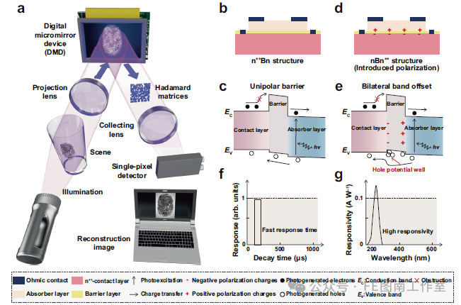
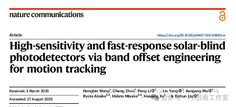
Figure 1: (a) Illustration of a single-pixel imaging system, detailing its primary components including the light source, target object, digital micromirror device, and a detector. The diagrams illustrate the device structure (b) and carrier dynamic process (c) in nBn++ junctions without polarization charges at the interfaces. The diagrams illustrate the device structure (d) and carrier dynamic processes (e) in nBn++ junctions with polarization charges at the interfaces. Fast response speed (f) and high responsivity (g) of a solar-blind photodetector that are required for single-pixel imaging application.
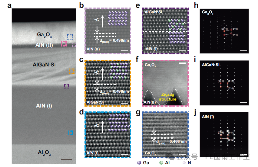
Figure 2 (a) AC‒TEM image of the Ga2O3/AlN (Ⅱ)/AlGaN:Si/AlN (Ⅰ) stack on a c-plane sapphire substrate. Scale bar, 200 nm. High-magnification AC‒TEM images of the upper AlN (II) layer (b), AlGaN:Si layer (c) and bottom AlN (I) layer (d), respectively. Atomic arrangement diagrams inserted in highlight the N-polarity of the nitrides. The dashed white lines indicate the interplanar spacings corresponding to (001) of AlN. e High-magnification AC‒TEM image of the AlGaN:Si/AlN (I) interface area, illustrating that the AlGaN:Si layer maintains the N-polarity of the AlN (I) template. Scale bar, 1 nm. High-magnification AC‒TEM image of the Ga2O3/AlN (II) interface area (f) and Ga2O3 layer (g), showing a zigzag structure in AlN (II)-assisted nucleation growth model in Ga2O3. Scale bars, 5 nm (f); 1nm (g). FFT patterns of the Ga2O3 (h), AlGaN:Si (i), and AlN (I) layers (j). Scale bars, 5 nm‒1.
Figure 3 (a) Schematic illustration of the Ga2O3/AlN/AlGaN:Si photodetector. Semi-logarithmic plots of the current-voltage (b) and current-time characteristics (c) in the dark and under illumination with varying intensities of 245 nm light. d Wavelength-dependent responsivity of the device at 0 V, with the semi-logarithmic representation provided in the inset. e Transient photoresponse characteristic curve obtained using a 248 nm pulsed laser at 0 V. The inset shows the response rise time curve. f Comparison of responsivity and fall time of the Ga2O3/AlN/AlGaN:Si photodetector with those of Ga2O3 and AlGaN p‒n, n‒n, and Schottky junction solar-blind photodetectors.
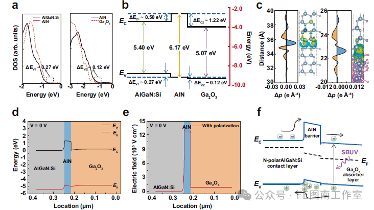
Figure 4 (a) Density of states (DOS) for AlGaN:Si and AlN, and AlN and Ga2O3. (b) Band alignment of AlGaN:Si/AlN and AlN/Ga2O3 interfaces in the absence of polarization effects. c Charge displacement and charge differences curves of the AlGaN:Si/AlN and AlN/Ga2O3 interfaces. Energy band diagram (d) and electric field profile (e) across the Ga2O3/AlN/AlGaN:Si heterojunction under the polarization. f Energy band diagram illustrating the photodetection mechanism of the Ga2O3/AlN/AlGaN:Si heterojunction.
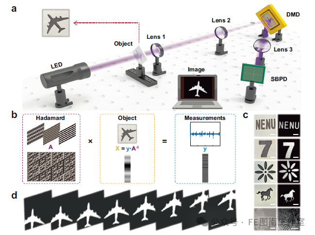
Figure 5 (a) Illustration of the experimental setup for single-pixel imaging. (b) Principle of single-pixel imaging, utilizing the Hadamard matrix for light field modulation. c Imaged samples (left) including the letter “NENU”, the number “7”, and patterns of “flower”, “horse”, and “fingerprint”, along with their corresponding reconstructed 256 × 256-pixel images (right). Scale bars, 3 mm. d Real-time imaging of a moving “airplane” with a resolution of 64 × 64 pixels. Scale bars, 3 mm.
Link:
https://doi.org/10.1038/s41467-025-63683-w
