Paper Sharing
【International Papers】In situ patterned damage-free etching of three-dimensional structures in β-Ga₂O₃ using triethylgallium
日期:2025-09-08阅读:610
Researchers from the Arizona State University have published a dissertation titled "In situ patterned damage-free etching of three-dimensional structures in β-Ga2O3 using triethylgallium" in Journal of Applied Physics.
Abstract
In this work, we report on the anisotropic etching characteristics of β-Ga2O3 using triethylgallium (TEGa) performed in situ within an MOCVD chamber. At sufficiently high substrate temperatures, TEGa can act as a strong etchant for β-Ga2O3 utilizing the suboxide reaction between Ga and Ga2O3 [4 Ga(s) + Ga2O3 (s) → 3Ga2O (g)]. We observe that due to the monoclinic crystal structure of β-Ga2O3, TEGa etching on both (010) and (001) substrates is highly anisotropic in nature, in terms of both sidewall roughness and lateral etch rate. Smooth sidewalls are only obtained along crystal orientations that minimize sidewall surface energy. Utilizing this technique, we also demonstrate deep sub-micrometer fins with smooth sidewalls and high aspect ratios. Furthermore, we also demonstrate the damage-free nature of TEGa etching by fabricating Schottky diodes on the etched surface, which display no change in the net donor concentration.
Conclusion
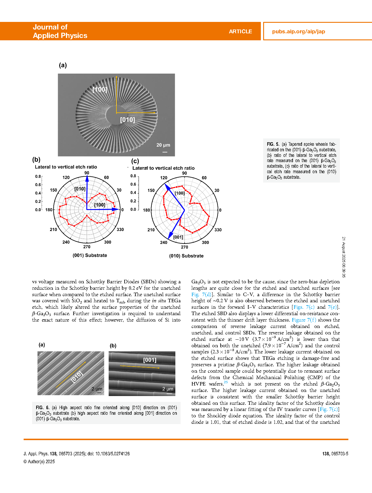
In conclusion, we studied the anisotropic dependence of TEGa etching on both the (001) and (010) oriented β-Ga2O3 substrates. We find that TEGa etching forms smooth sidewalls for features oriented along the [010] direction on (001)-β-Ga2O3 and along the [001] direction on (010)-β-Ga2O3. Smooth sidewalls are obtained due to the formation of (100) or (100) like sidewall planes with low surface energy. Furthermore, these two in-plane orientations also display the lowest lateral etch rates with a lateral to vertical etch rate ratio of ∼0.1, making them suitable for fabricating high aspect ratio 3-D structures. The damage-free nature of TEGa etching was also confirmed using electrical measurements on Ni-SBDs fabricated on the etched surface, which showed no change in the net donor concentration (ND − NA). This work enhances our understanding of the in situ TEGa etching and paves the way for the development of highly scaled vertical and lateral three-dimensional devices in β-Ga2O3.
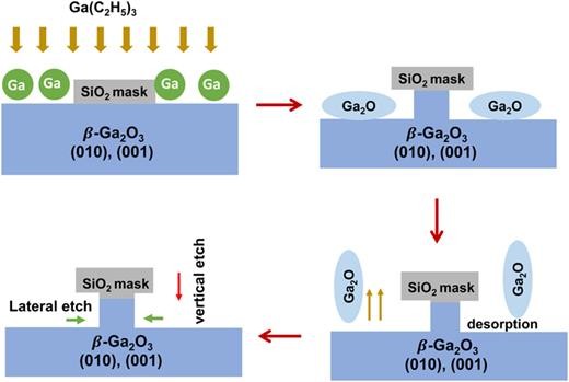
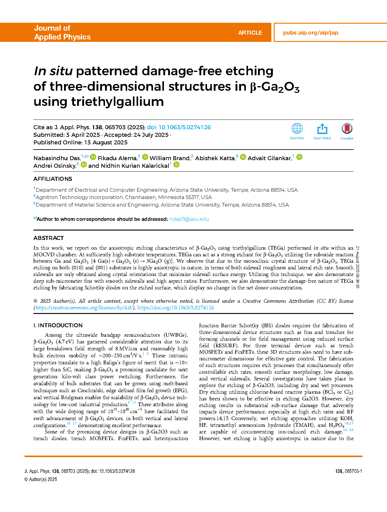
FIG.1 Schematic of the MOCVD based etching of β-Ga2O3 using triethylgallium.
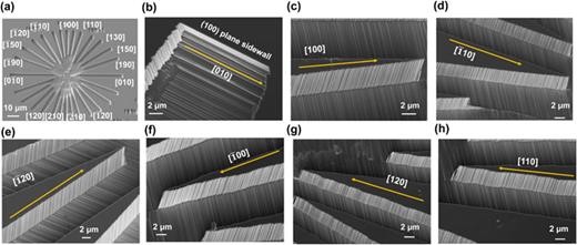
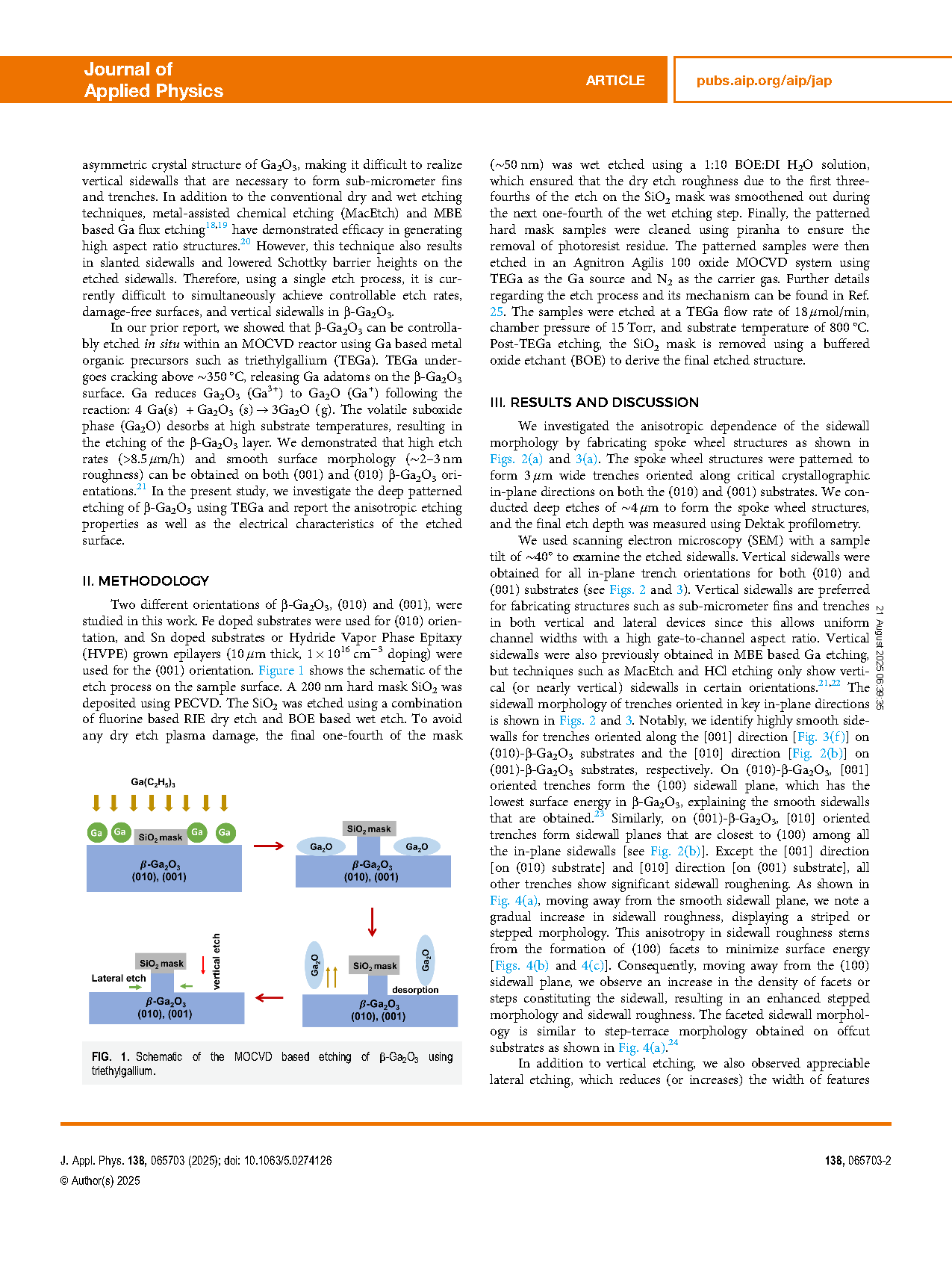
FIG.2 (a) Spoke wheel structure for the (001) β-Ga2O3 substrate. (b)–(h) Sidewall morphology for fins in different directions.
DOI:
doi.org/10.1063/5.0274126