Paper Sharing
【International Papers】Current Status of Bulk β-Ga₂O₃ and β-(AlₓGa₁₋ₓ)₂O₃ Crystal Growth
日期:2025-09-08阅读:697
Researchers from the Leibniz-Institut für Kristallzüchtung (IKZ) have published a dissertation titled "Current Status of Bulk β-Ga2O3 and β-(AlxGa1-x)2O3 Crystal Growth" in IEEE Transactions on Semiconductor Manufacturing.
Background
β-Ga₂O₃, as an ultra-wide bandgap semiconductor (~4.8 eV), is regarded as a core candidate material for next-generation power electronic devices and deep-ultraviolet photodetectors due to its extremely high breakdown electric field and excellent thermochemical stability. The development of large-size, high-quality β-Ga₂O₃ bulk single crystals is a prerequisite for its industrial applications. At present, melt growth methods (EFG, CZ, VB, DS, etc.) and vapor-phase methods are mainly employed for crystal growth, but these techniques differ in terms of crystal size, quality, and cost. Alloying (β-(AlₓGa₁₋ₓ)₂O₃) provides a new material pathway with tunable bandgap, enabling applications in high-frequency devices and solar-blind detection; however, the stable growth of large-size crystals is still in its early stage.
Abstract
β-Ga2O3 and its solid solutions β-(AlxGa1-x)2O3 are considered as potential candidate materials for next generation power devices due to their ultra-wide bandgaps (4.85–5.6 eV) and large breakdown electric field (≥8 MVcm-1). Wafers prepared from bulk crystals constitute a foundation in a device fabrication chain. The present report briefly discusses thermodynamics, challenges in growing bulk crystals from the melt by different methods, which enable at least 2-inch diameter wafers, crystal structural quality, electrical properties, and factors affecting crystal growth costs.
Conclusion
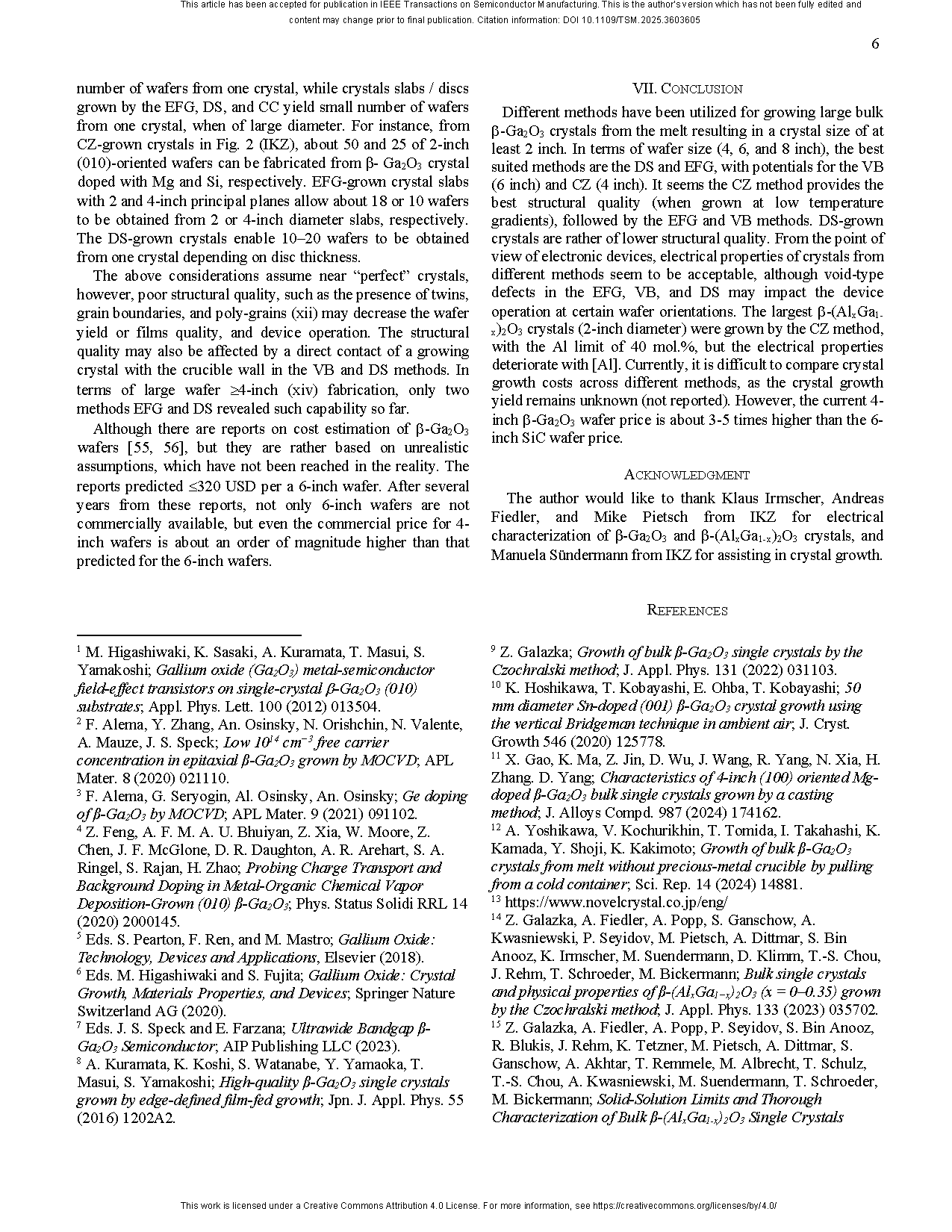
Different methods have been utilized for growing large bulk β-Ga2O3 crystals from the melt resulting in a crystal size of at least 2 inch. In terms of wafer size(4, 6, and 8 inch), the best suited methods are the DS and EFG, with potentials for the VB(6 inch) and CZ (4 inch). It seems the CZ method provides the best structural quality (when grown at low temperature gradients), followed by the EFG and VB methods. DS-grown crystals are rather of lower structural quality. From the point of view of electronic devices, electrical properties of crystals from different methods seem to be acceptable, although void-type defects in the EFG, VB, and DS may impact the device operation at certain wafer orientations. The largest β-(AlxGa1-x)2O3 crystals (2-inch diameter) were grown by the CZ method, with the Al limit of 40 mol.%, but the electrical properties deteriorate with [Al]. Currently, it is difficult to compare crystal growth costs across different methods, as the crystal growth yield remains unknown (not reported). However, the current 4-inchβ-Ga2O3 wafer price is about 3-5 times higher than the 6 inch SiC wafer price.
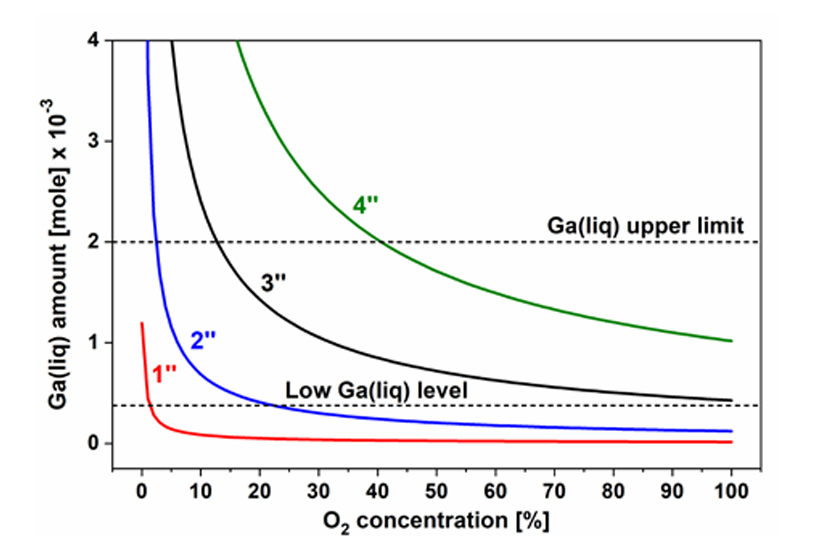
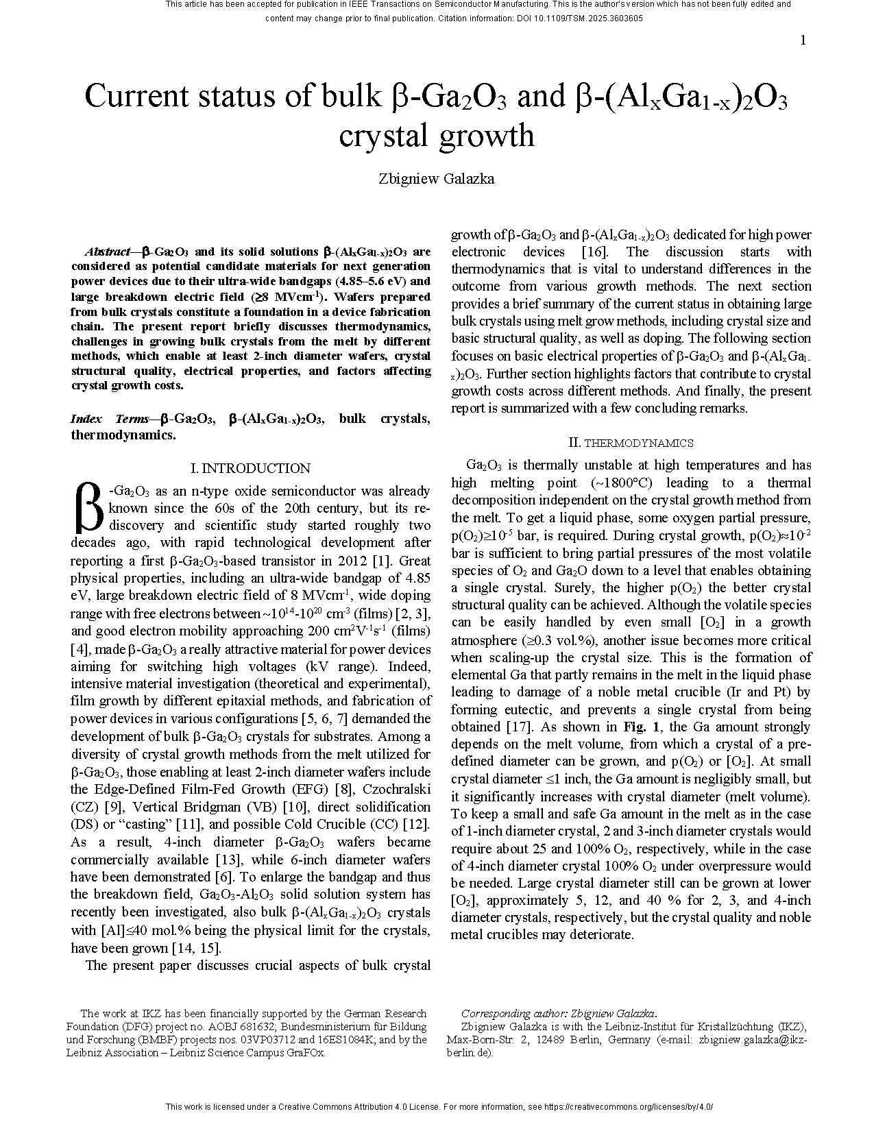
Fig. 1. Amount of elemental gallium formed in the β-Ga2O3 melt versus O2 concentration in the growth atmosphere depending on crystal diameter (in inch). The dashed lines correspond to a safe level and upper limit, respectively.
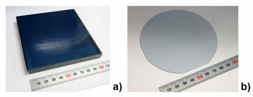
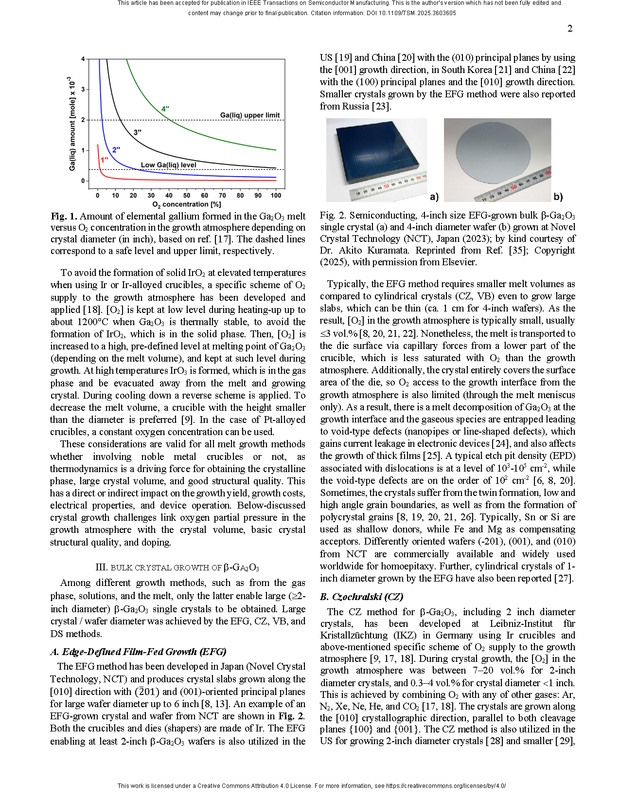
Fig. 2. Semiconducting, 4-inch size EFG-grown bulk β-Ga2O3 single crystal (a) and 4-inch diameter wafer (b)
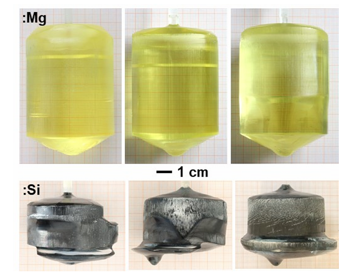
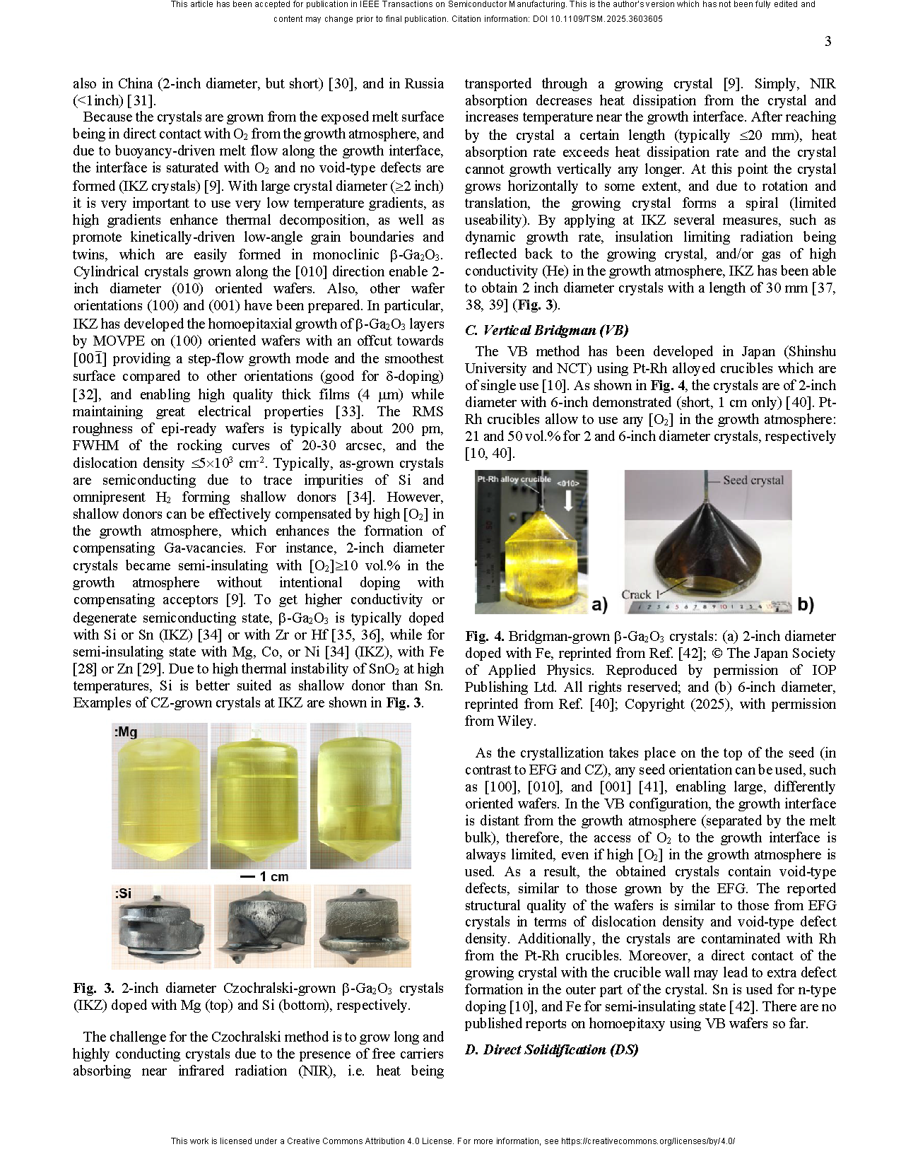
Fig. 3. 2-inch diameter Czochralski-grown β-Ga2O3 crystals (IKZ) doped with Mg (top) and Si (bottom), respectively.
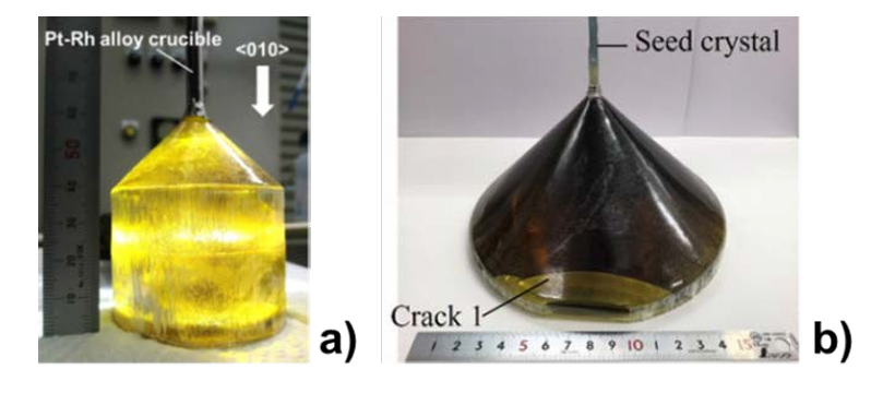
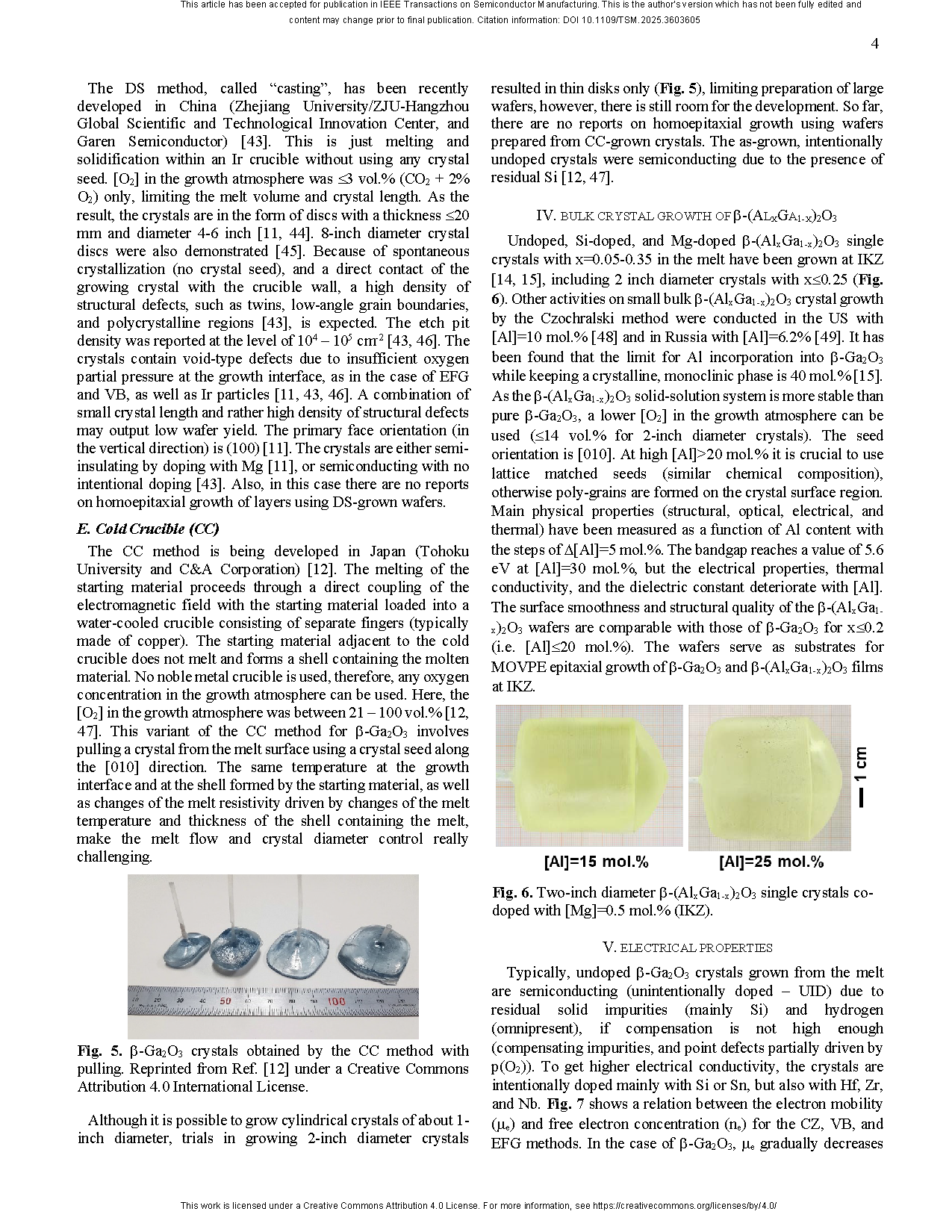
Fig. 4. Bridgman-grown β-Ga2O3 crystals: (a) 2-inch diameter doped with Fe, and (b) 6-inch diameter.
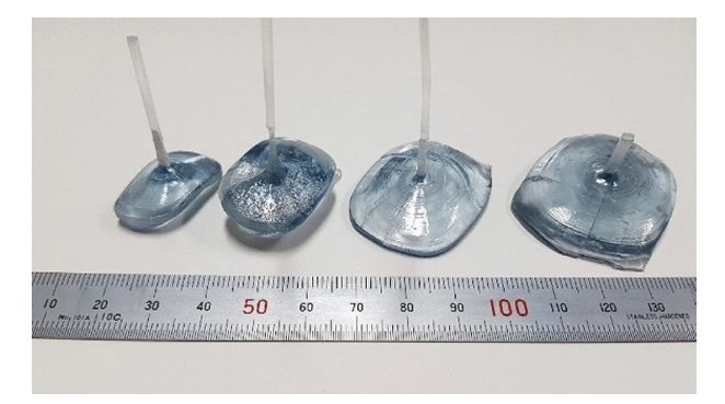
Fig. 5. β-Ga2O3 crystals obtained by the CC method with pulling.
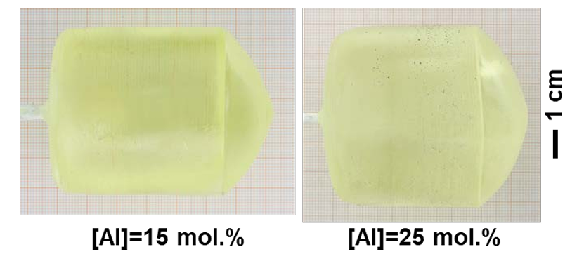
Fig. 6. Two-inch diameter β-(AlxGa1-x)2O3 single crystals co-doped with [Mg]=0.5 mol.% (IKZ).
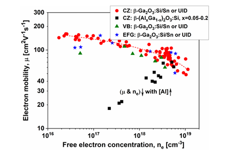
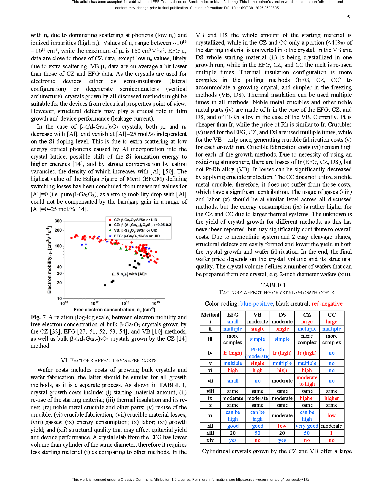
Fig. 7. A relation (log-log scale) between electron mobility and free electron concentration of bulk β-Ga2O3 crystals grown by the CZ.
DOI:
doi.org/10.1109/TSM.2025.3603605