Paper Sharing
【International Papers】Versatile Contact Engineering on β-Ga₂O₃ Using EGaIn for Schottky Diodes and MESFET Applications
日期:2025-09-09阅读:651
Researchers from the Yonsei University have published a dissertation titled "Versatile Contact Engineering on β-Ga2O3 Using EGaIn for Schottky Diodes and MESFET Applications" in Advanced Electronic Materials.
Background
Gallium oxide (Ga2O3) is well well-known polymorphism material, which has five crystalline phases of α, β, γ, δ, and ε. Among them, beta gallium oxide (β-Ga2O3), an ultra-wide bandgap (UWB, 4.8 eV) semiconductor, is a very promising n-type active channel material in future electronics such as 5G and AI technologies due to its excellent electrical and optical properties. From these reasons, many researchers focused on the β-Ga2O3 to achieve higher power efficiency at high voltages and high temperatures, and to reduce energy waste for zero carbon emission. However, β-Ga2O3 has been reported to be difficult to form proper Ohmic contact with former metal electrodes, through metal deposition and lift-off processes based on conventional thin film technology. To solve this problem, plasma etching and post-thermal treatment processes are necessary to achieve good Ohmic contact properties on β-Ga2O3. Because these additional processes could create oxygen vacancies (VOs), and the generated VO acted as a donor (donated electron) by increasing the electron concentration at the β-Ga2O3 channel surface. As a result, the electron doping effect brings good Ohmic contact properties at the interface of β-Ga2O3 and deposited metal electrodes.
Abstract
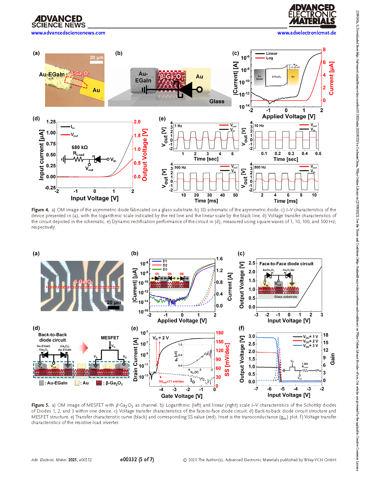
Beta gallium oxide (β-Ga2O3) has emerged as a promising ultrawide bandgap n-type semiconductor for large-area circuit integration and high-power device applications in the field of 5G and AI technology. However, β-Ga2O3 has a critical problem in Ohmic contact formation using a traditional metallization method. In this study, a low-temperature fabrication strategy is successfully demonstrated of an Ohmic contact electrode, employing eutectic gallium indium (EGaIn) liquid metal on β-Ga2O3 active channel material for Schottky diode circuit and metal semiconductor field effect transistor (MESFET) applications. The selective screen-printing of Ohmic and rectifying contacts enables monolithic integration of symmetric and asymmetric device architectures, including source/drain electrodes, Schottky diodes, and FETs without additional post-thermal annealing and etching processes. The β-Ga2O3/Au Schottky diodes exhibit good rectifying properties of a current on/off ratio of 10⁷ and an ideality factor (η) of 1.63, while the MESFET devices demonstrate a drain current on/off ratio of ≈3.1 × 10⁶.
Conclusion
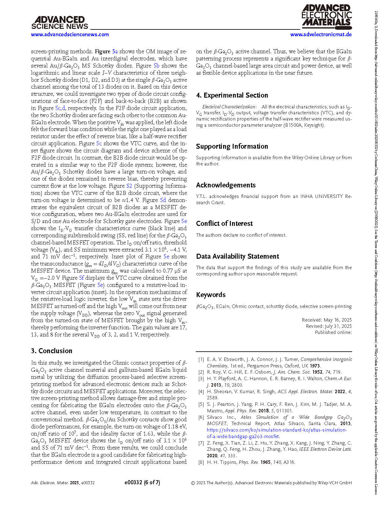
In this study, we investigated the Ohmic contact properties of β-Ga2O3 active channel material and gallium-based EGaIn liquid metal by utilizing the diffusion process-based selective screen-printing method for advanced electronic devices such as Schottky diode circuits and MESFET applications. Moreover, the selective screen-printing method allows damage-free and simple processing for fabricating the EGaIn electrodes onto the β-Ga2O3 active channel, even under low temperature, in contrast to the conventional method. β-Ga2O3/Au Schottky contacts show good diode performances, for example, the turn-on voltage of 1.18 eV, on/off ratio of 107, and the ideality factor of 1.63, while the β-Ga2O3 MESFET device shows the ID on/off ratio of 3.1 × 10⁶ and SS of 71 mV dec−1. From these results, we could conclude that the EGaIn electrode is a good candidate for fabricating high-performance devices and integrated circuit applications based on the β-Ga2O3 active channel. Thus, we believe that the EGaIn patterning process represents a significant key technique for β-Ga2O3 channel-based large area circuit and power device, as well as flexible device applications in the near future.
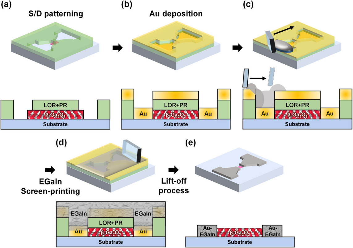
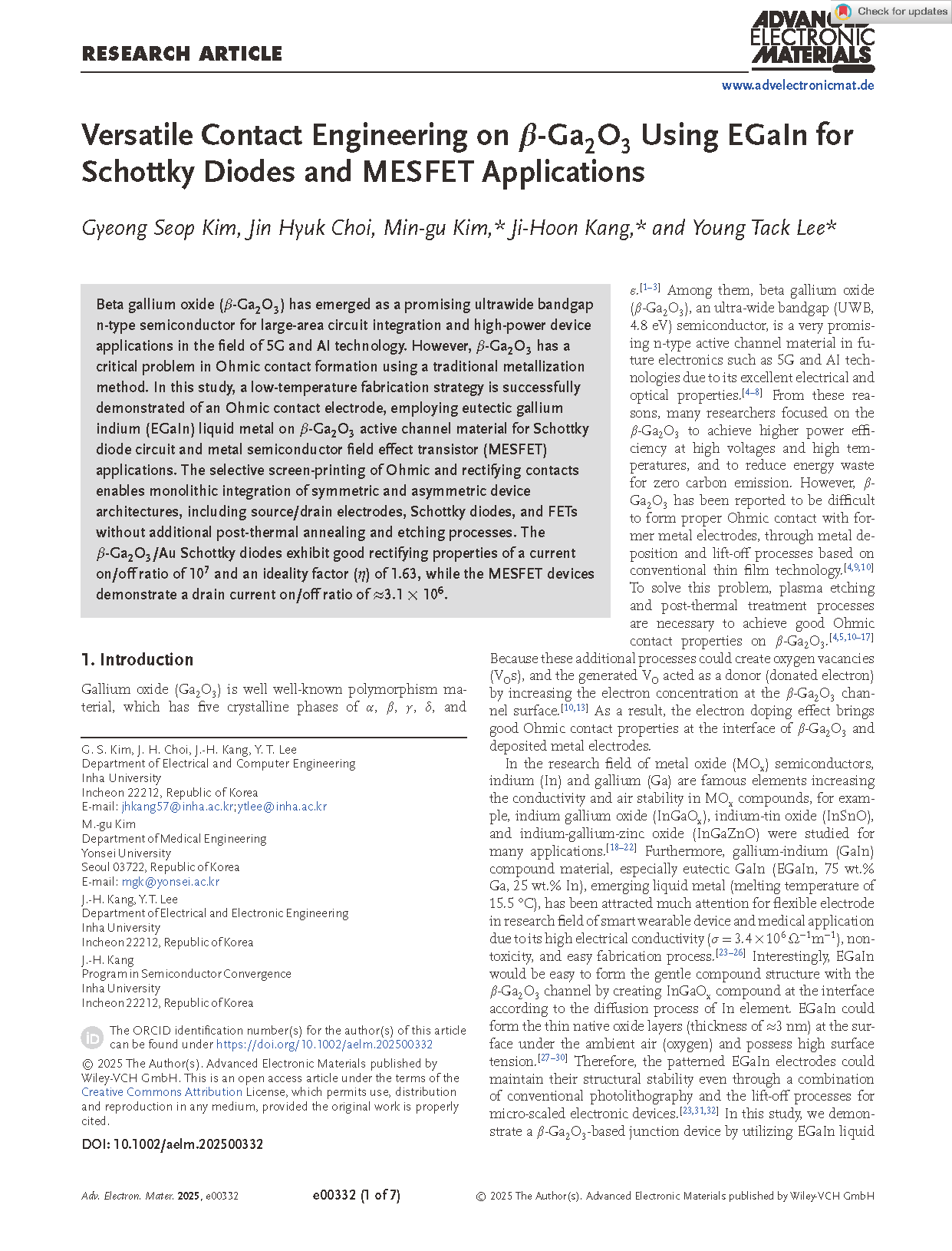
Figure 1.The schematic design (diagonal view and cross-section) fabrication processes of EGaIn S/D electrodes by using photolithography and lift-off process. a) Schematic of the after spin-coating PR and LOR. b) Schematic after Au sputtering for the buffer layer on β-Ga2O3. c) Schematic of fabricating EGaIn with a PDMS brush. d) The gradual diffusion of EGaIn into Au over time. e) Schematic after the lift-off process with acetone.
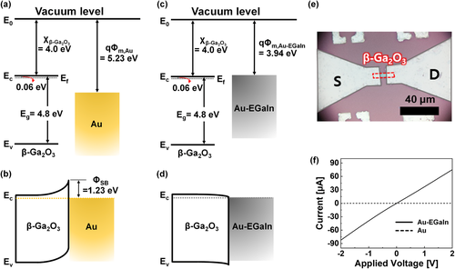
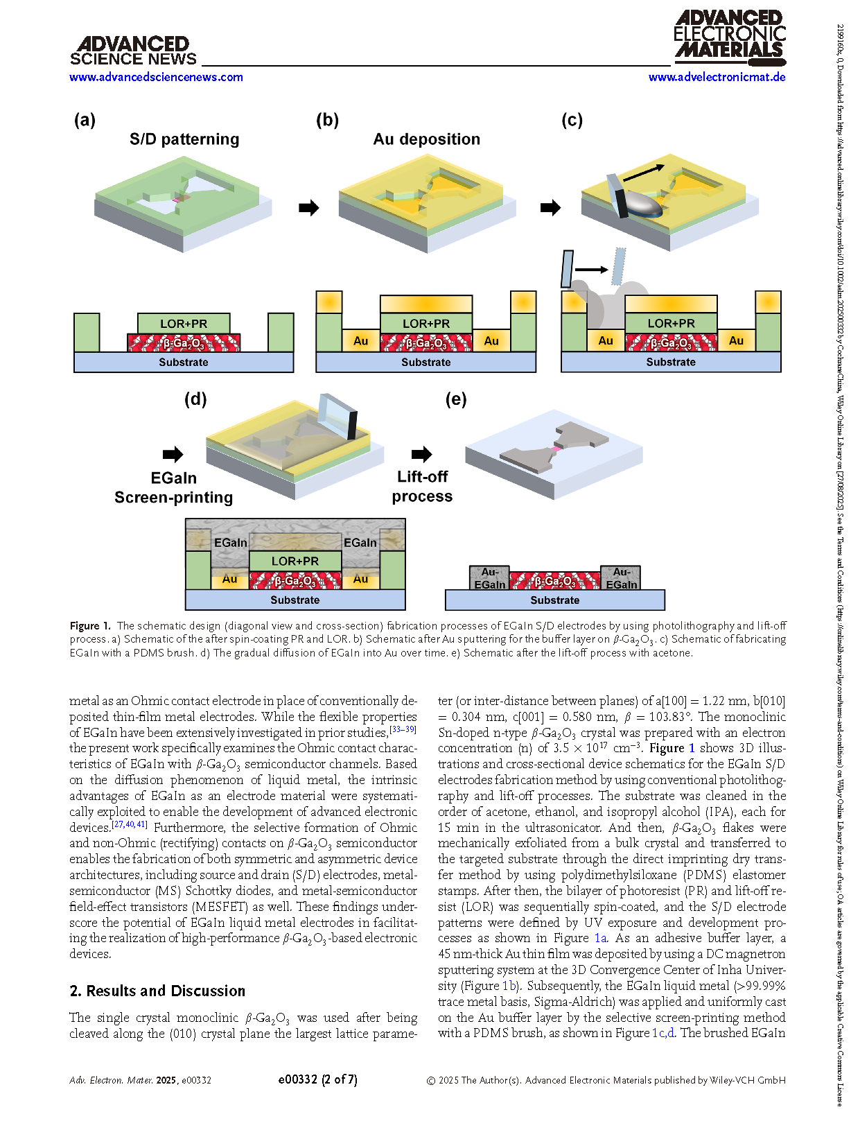
Figure 2.a) Energy Band diagram of β-Ga2O3, Au, Au-EGaIn (before junction). b) Energy band diagrams of β-Ga2O3/Au Schottky contact. c) Energy Band diagram of β-Ga2O3, Au-EGaIn (before junction). d) Energy band diagrams of Au-EGaIn/β-Ga2O3 Ohmic contact. e) OM image and f) I–V characteristics curves of β-Ga2O3 channel-based symmetric devices of β-Ga2O3/Au Schottky (dashed line) and Au-EGaIn/ β-Ga2O3 Ohmic contact (Solid line).
DOI:
doi.org/10.1002/aelm.202500332