Paper Sharing
【International Papers】Design of CsSnBr₃/Ga₂O₃ Hybrid Photodetectors for High UV Selectivity and Bifacial Usage
日期:2025-09-10阅读:617
Researchers from the University of Parma have published a dissertation titled " Design of CsSnBr3/Ga2O3 Hybrid Photodetectors for High UV Selectivity and Bifacial Usage" in Advanced Theory and Simulations.
Abstract
The operation and characteristics of a novel all-inorganic hybrid p–n heterojunction, formed by lead-free perovskite CsSnBr3deposited on Ga2O3, are numerically investigated. Key performance parameters such as current–voltage behavior, quantum efficiency (QE), spectral responsivity (R), detectivity (D*), noise-equivalent power (NEP), and band alignment are analyzed. Results show a high illumination-to-dark current ratio of 10⁷ and a rectification ratio of ≈7.6 × 10⁶ (in dark) and 1.33 × 10⁴ (under illumination) at ±3 V. The CsSnBr3/Ga2O3 photodetector supports bifacial, self-powered, solar-blind, and ultraviolet-visible (UV–Vis) detection modes by adjusting layer thickness and doping concentration. In selective UV mode, it achieves a responsivity of 57.5 mA/W, detectivity of 3.6 × 10¹⁰ Jones, and noise-equivalent power of 9.84 × 10⁻¹² W/. In the UV–Vis mode, these improve to 161 mA/W, 1 × 10¹¹ Jones, and 3.51 × 10⁻¹³ W/, respectively. The device also shows an effective visible-light detection upon reversing the illumination direction, indicating potential use in stacked solar cells. This study outlines critical design parameters and optimization strategies, paving the way for future research on stable, lead-free, all-inorganic hybrid devices combining perovskites with wide-bandgap semiconductors.
Conclusion
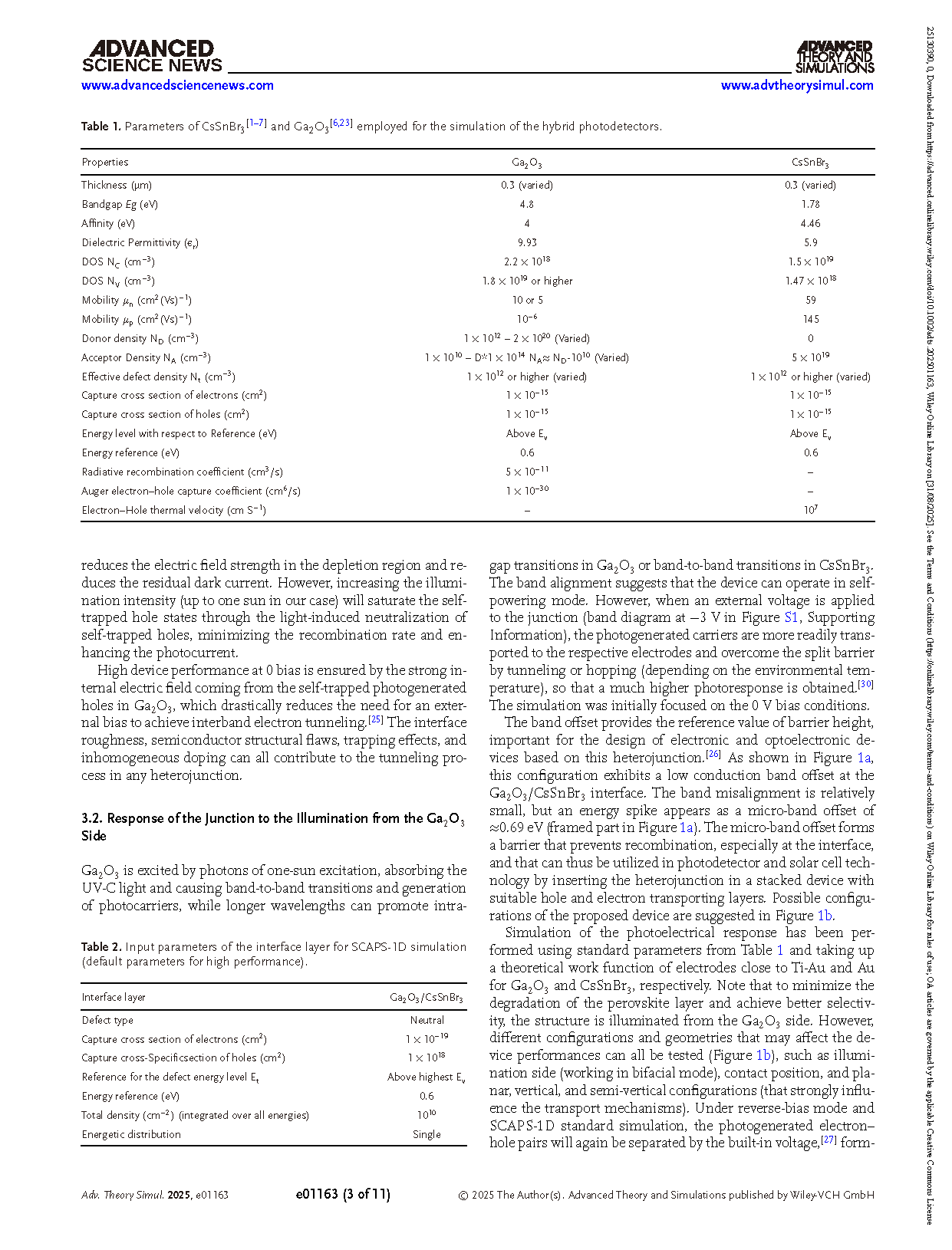
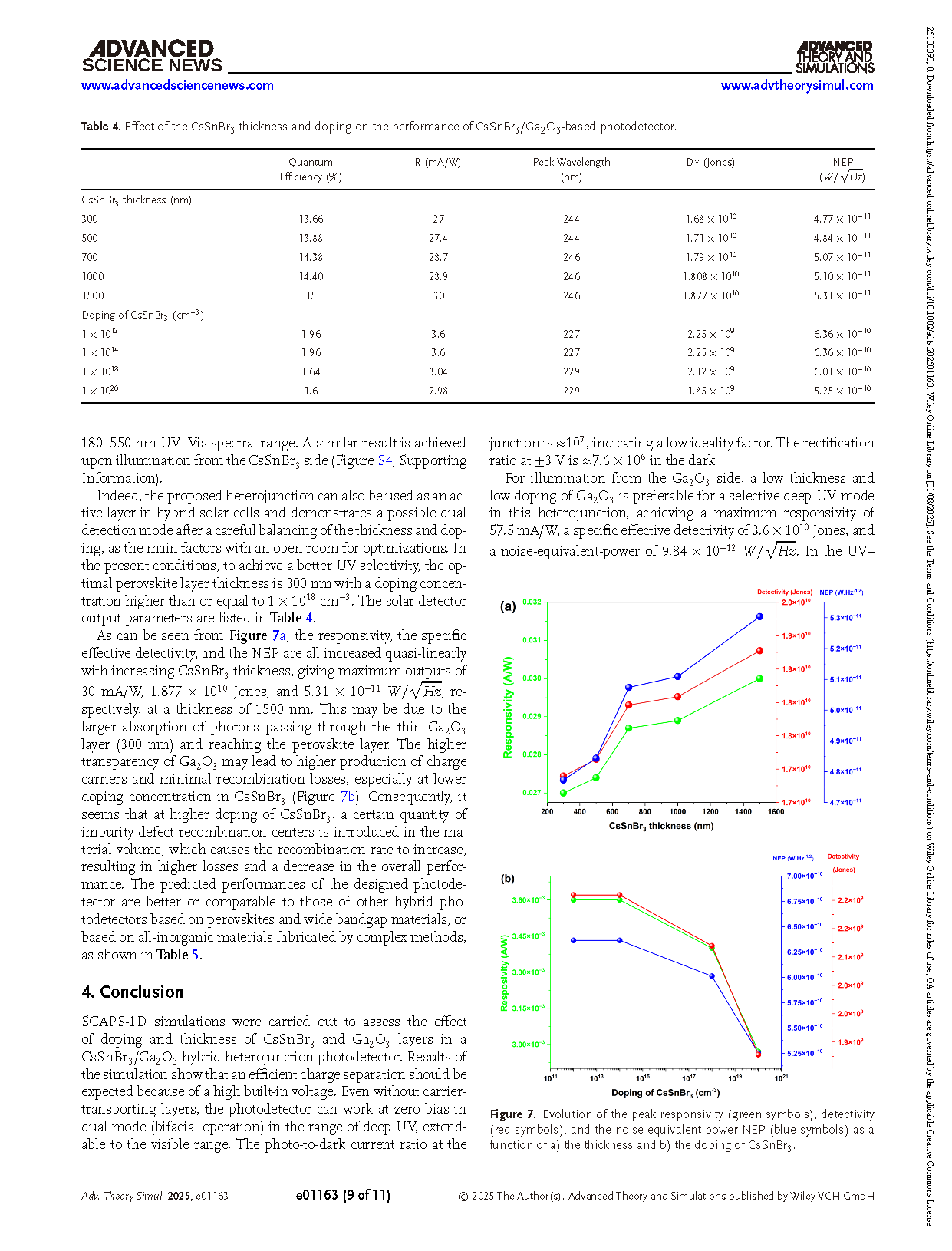
SCAPS-1D simulations were carried out to assess the effect of doping and thickness of CsSnBr3 and Ga2O3 layers in a CsSnBr3/Ga2O3 hybrid heterojunction photodetector. Results of the simulation show that an efficient charge separation should be expected because of a high built-in voltage. Even without carrier-transporting layers, the photodetector can work at zero bias in dual mode (bifacial operation) in the range of deep UV, extendable to the visible range. The photo-to-dark current ratio at the junction is ≈107, indicating a low ideality factor. The rectification ratio at ±3 V is ≈7.6 × 10⁶ in the dark.
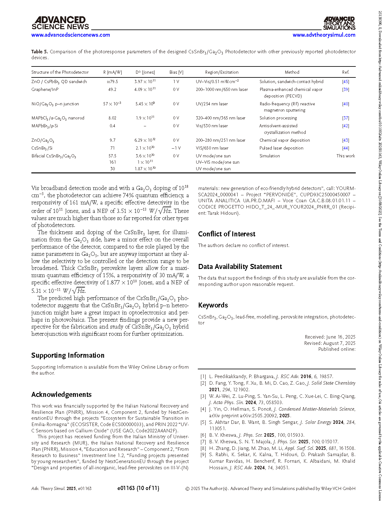
For illumination from the Ga2O3 side, a low thickness and low doping of Ga2O3 is preferable for a selective deep UV mode in this heterojunction, achieving a maximum responsivity of 57.5 mA/W, a specific effective detectivity of 3.6 × 10¹⁰ Jones, and a noise-equivalent-power of 9.84 × 10⁻¹² W/. In the UV–Vis broadband detection mode and with a Ga2O3 doping of 1018 cm−3, the photodetector can achieve 74% quantum efficiency, a responsivity of 161 mA/W, a specific effective detectivity in the order of 1011 Jones, and a NEP of 3.51 × 10⁻¹³ W/. These values are much higher than those so far reported for other types of photodetectors.
The thickness and doping of the CsSnBr3 layer, for illumination from the Ga2O3 side, have a minor effect on the overall performance of the detector, compared to the role played by the same parameters in Ga2O3, but are anyway important as they allow the selectivity to be controlled or the detection range to be broadened. Thick CsSnBr3 perovskite layers allow for a maximum quantum efficiency of 15%, a responsivity of 30 mA/W, a specific effective detectivity of 1.877 × 10¹⁰ Jones, and a NEP of 5.31 × 10⁻¹¹ W/.
The predicted high performance of the CsSnBr3/Ga2O3 photodetector suggests that the CsSnBr3/Ga2O3 hybrid p–n heterojunction might have a great impact in optoelectronics and perhaps in photovoltaics. The present findings provide a new perspective for the fabrication and study of CsSnBr3/Ga2O3 hybrid heterojunction with significant room for further optimization.
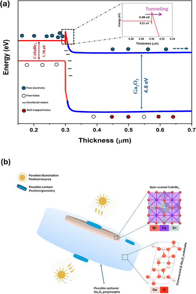
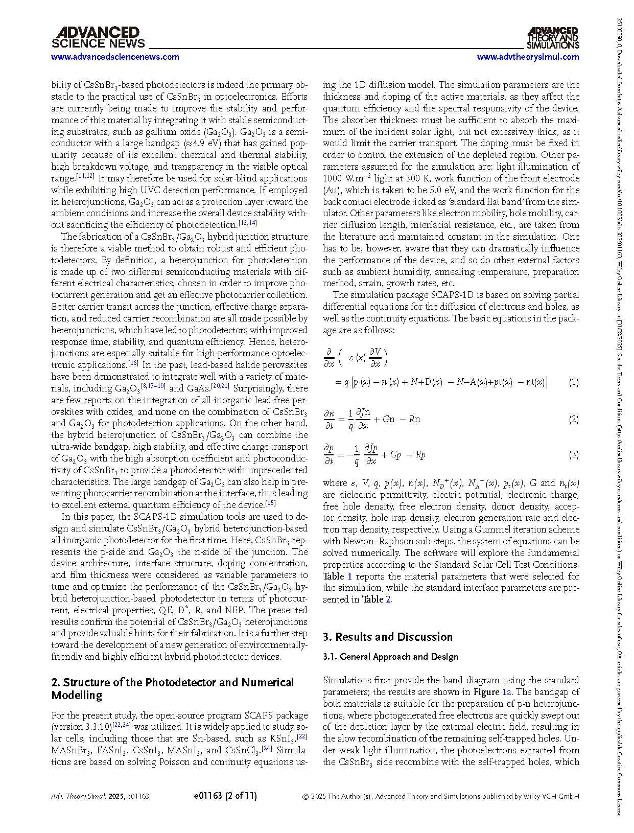
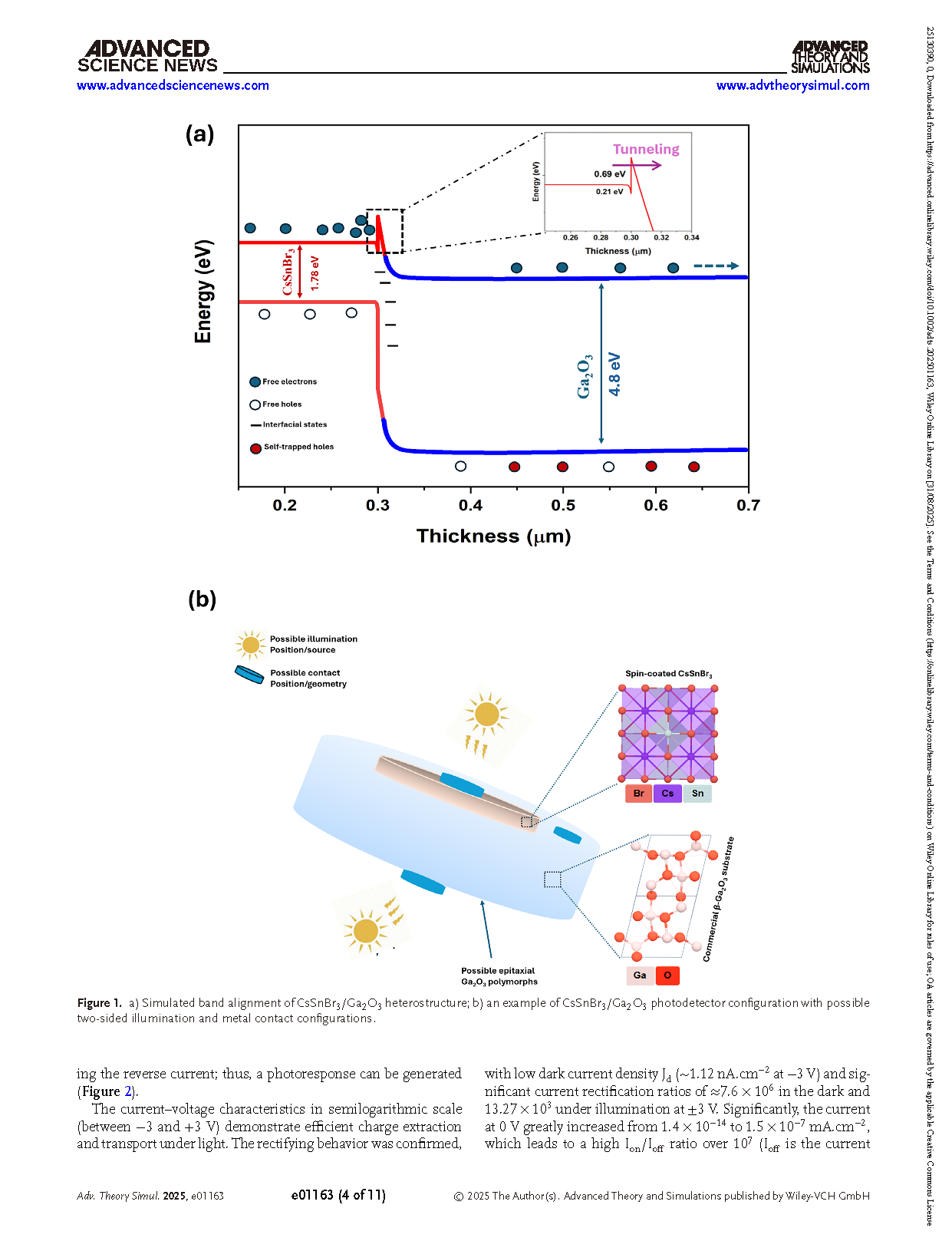
Figure 1 a) Simulated band alignment of CsSnBr3/Ga2O3 heterostructure; b) an example of CsSnBr3/Ga2O3 photodetector configuration with possible two-sided illumination and metal contact configurations.
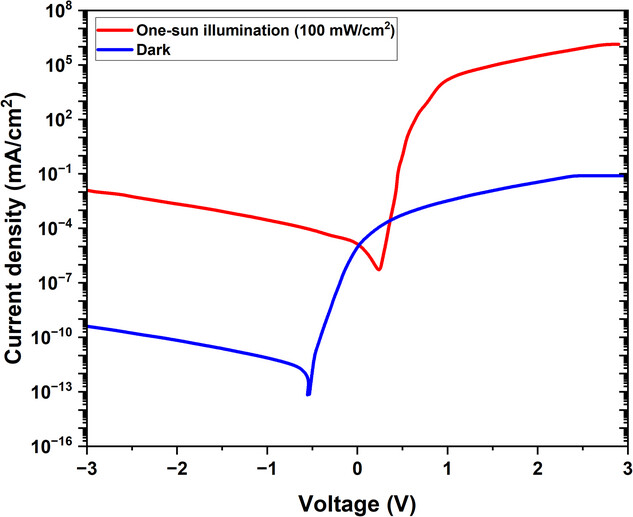
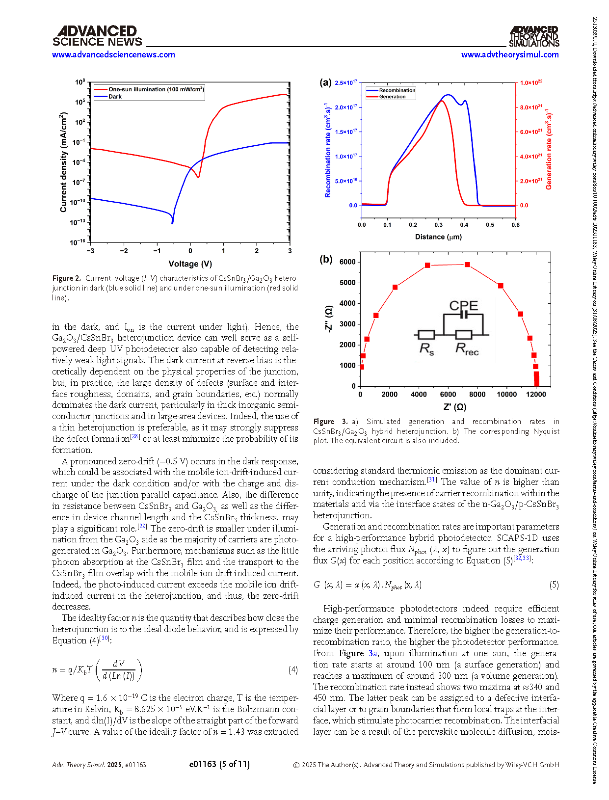
Figure 2 Current–voltage (I–V) characteristics of CsSnBr3/Ga2O3 heterojunction in dark (blue solid line) and under one-sun illumination (red solid line).
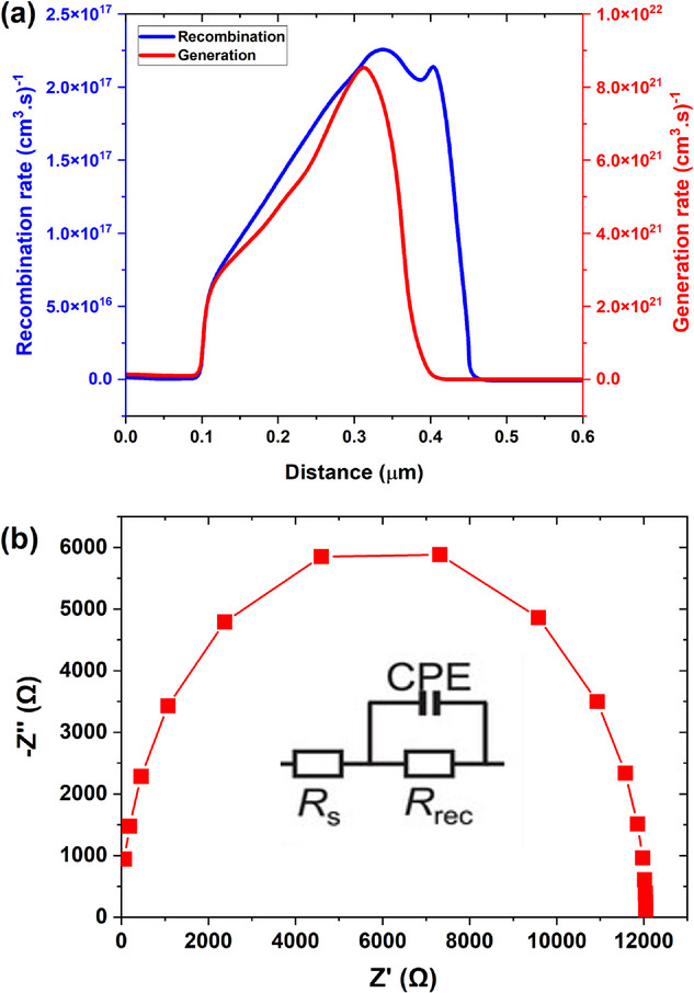
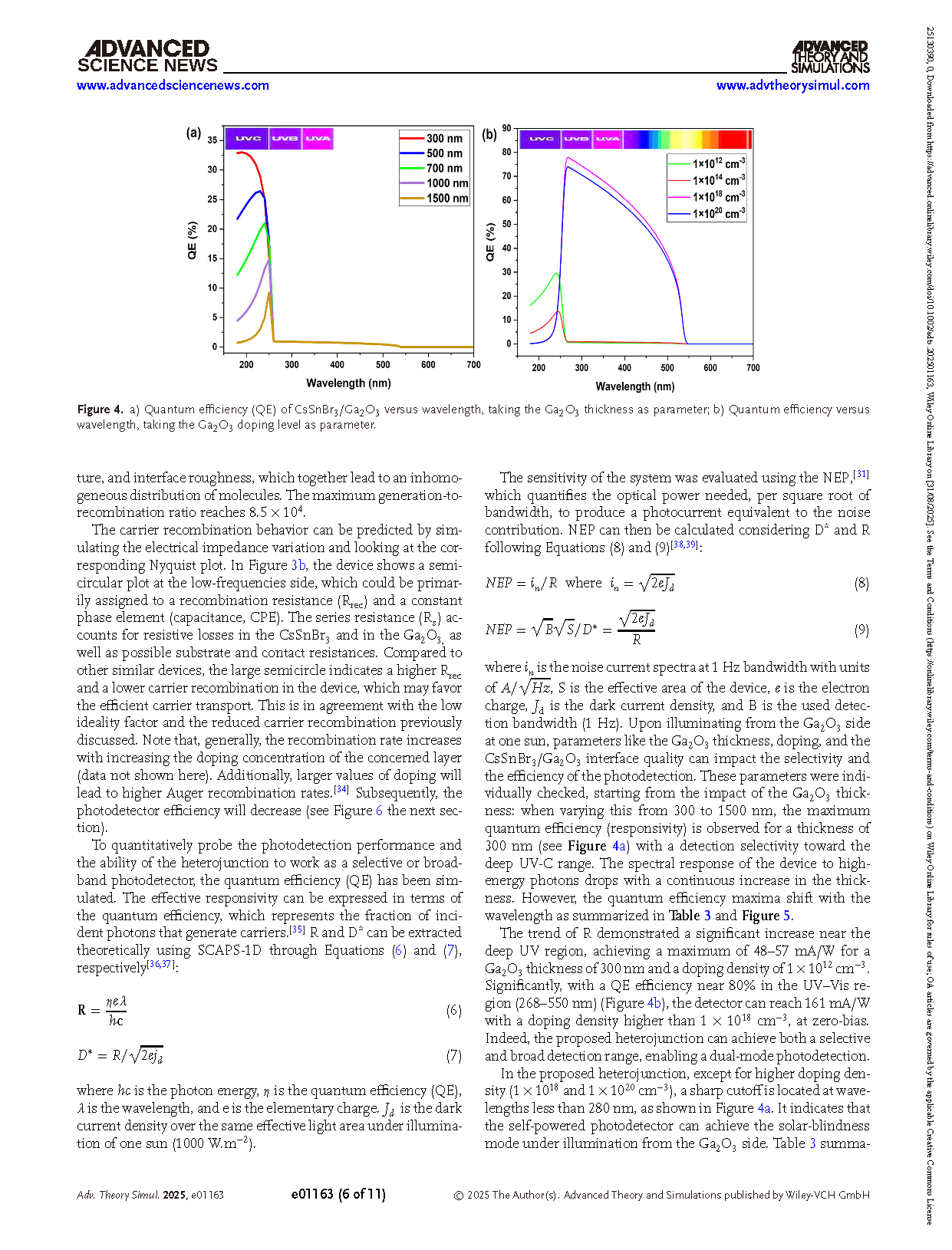
Figure 3 a) Simulated generation and recombination rates in CsSnBr3/Ga2O3 hybrid heterojunction. b) The corresponding Nyquist plot. The equivalent circuit is also included.
DOI:
doi.org/10.1002/adts.202501163