Paper Sharing
【Member Papers】Optimizing transparency, conductivity, and luminescence in Eu-(Ga,In)₂O₃ thin films via oxygen pressure control
日期:2025-09-10阅读:605
Researchers from the Guilin University of Electronic Technology have published a dissertation titled "Optimizing transparency, conductivity, and luminescence in Eu-(Ga,In)2O3 thin films via oxygen pressure control" in Journal of Alloys and Compounds.
Project Support
This work was supported by Guangxi Science and Technology Plan Project (AD24010060, AA23023010), National Natural Science Foundation of China (No. 52262022,62205080,62174041, 62361022), Guangxi Key Guangxi Key Laboratory of Precision Navigation and Application (No. DH202202), Innovation Project of Guangxi Graduate Education(No.YCBZ2025153).
Background
Transparent conducting oxides (TCOs) are essential in optoelectronic devices, such as solar cells, light-emitting diodes (LEDs), and flat-panel displays, due to their unique combination of high optical transparency and electrical conductivity. Among TCOs, gallium-indium oxide (Ga-In-O) has emerged as a promising material due to its enhanced thermal stability, tunable electronic properties, and resistance to ionized impurity scattering. Studies have shown that doping indium oxide (In2O3) with gallium (Ga) to form Ga-In-O improves these characteristics while retaining key optical properties. These properties make Ga-In-O a strong candidate for advanced transparent conductive applications.
Abstract
We investigated the influence of oxygen partial pressure on the structural, optical, and electronic properties of Eu-(Ga,In)2O3 thin films grown by pulsed laser deposition (PLD). A key innovation of this work lies in demonstrating that transparency, conductivity, and photoluminescence can be simultaneously optimized by precisely controlling the oxygen pressure during deposition. Films deposited at 10 Pa exhibit high visible transparency (>88 %) and crystallinity, while those at 10−2 Pa show strong Eu3+ emission (∼610–620 nm) from the 5D0→7F2 transition. Structural analysis reveals a pressure-driven phase transition from amorphous to crystalline, accompanied by a shift in transport from trap-limited/percolation to band-like conduction. Temperature-dependent Hall measurements of the 10−1 Pa film confirm shallow donor activation with an extracted activation energy of 0.00049 eV. These findings offer a scalable approach for multifunctional tuning of rare-earth-doped oxide semiconductors, enabling their application in transparent electronics, optoelectronic devices, and photonic systems.
Highlights
● Eu-(Ga,In)2O3thin films were deposited by PLD under oxygen pressures.
● Oxygen pressure tunes structure, transparency, conductivity, and luminescence.
● 10 Pa gives high transparency; 10−2Pa shows strong Eu3+red photoluminescence.
● Crystallinity governs the transition from trap-limited to band-like conduction.
● Activation energy of 0.00049 eV extracted from the 10⁻¹ Pa temperature-dependent data.
Conclusion
This study demonstrates that Eu-(Ga,In)2O3 thin films fabricated via PLD exhibit tunable structural, optical, and electronic properties through precise control of oxygen partial pressure. By varying the oxygen pressure from 10−4 to 10 Pa, we achieved simultaneous optimization of three key performance metrics: high optical transparency (>88 %) at 10 Pa, strong red photoluminescence (∼610–620 nm) at 10−2 Pa due to the 5D0 →7F2 transition of Eu3+, and enhanced carrier mobility under intermediate pressures.
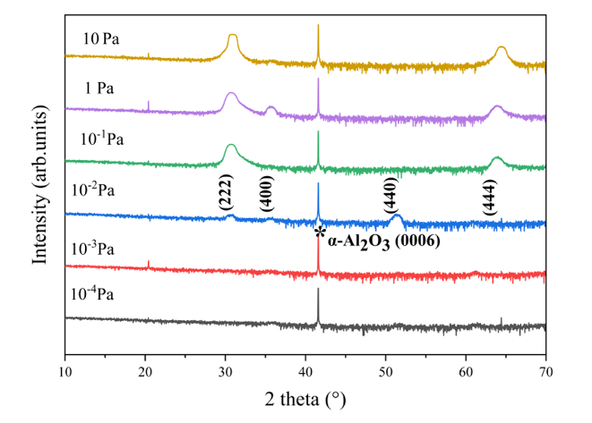
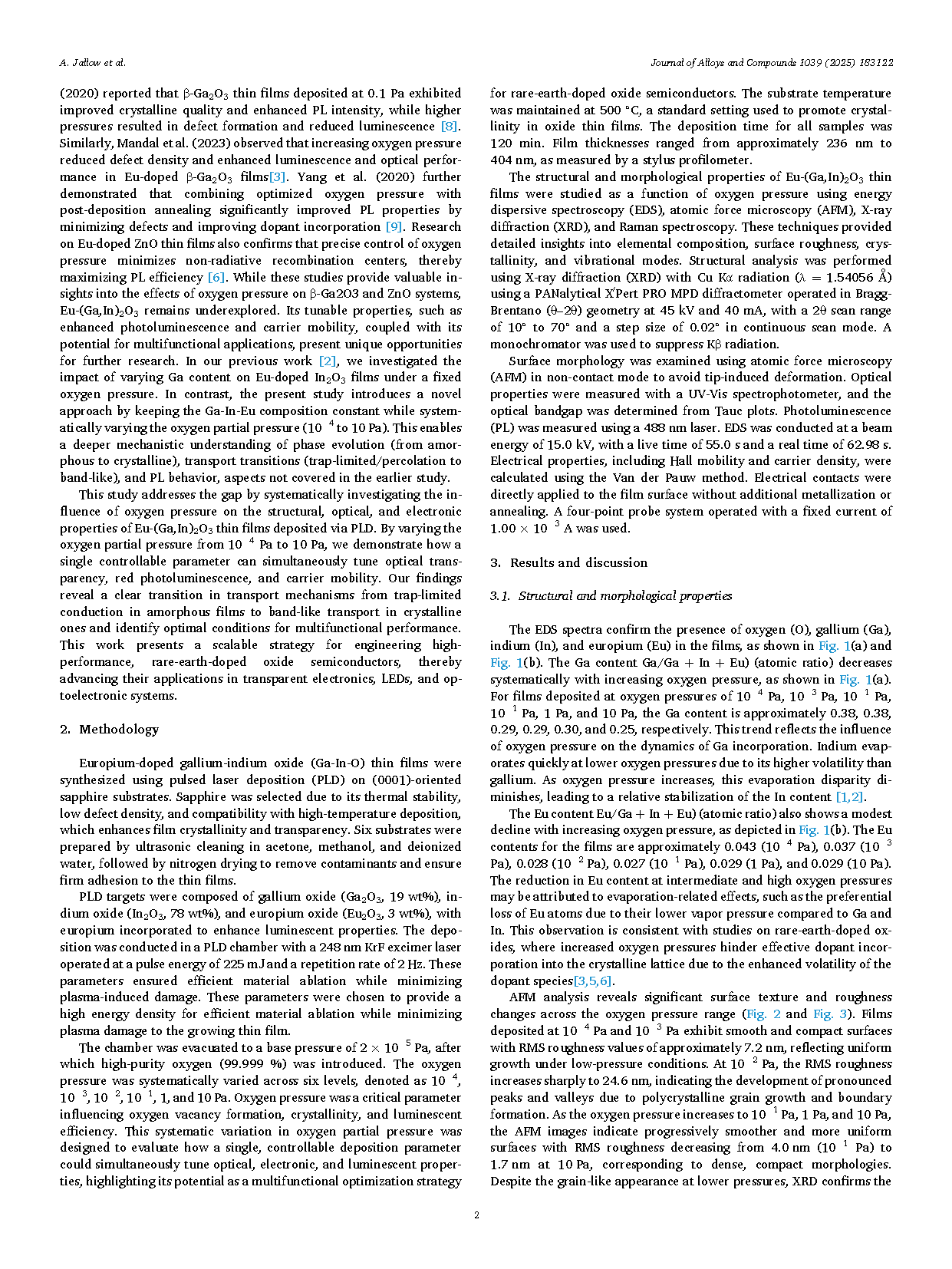
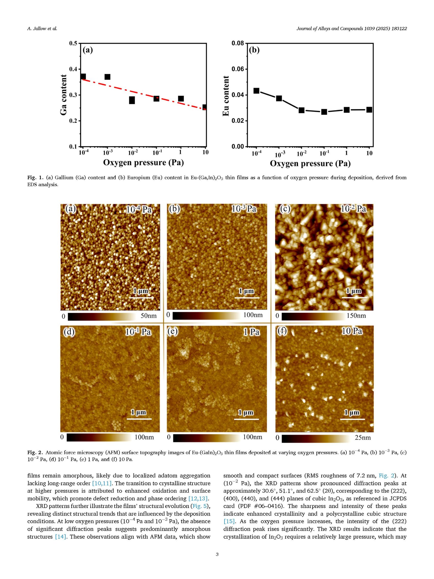
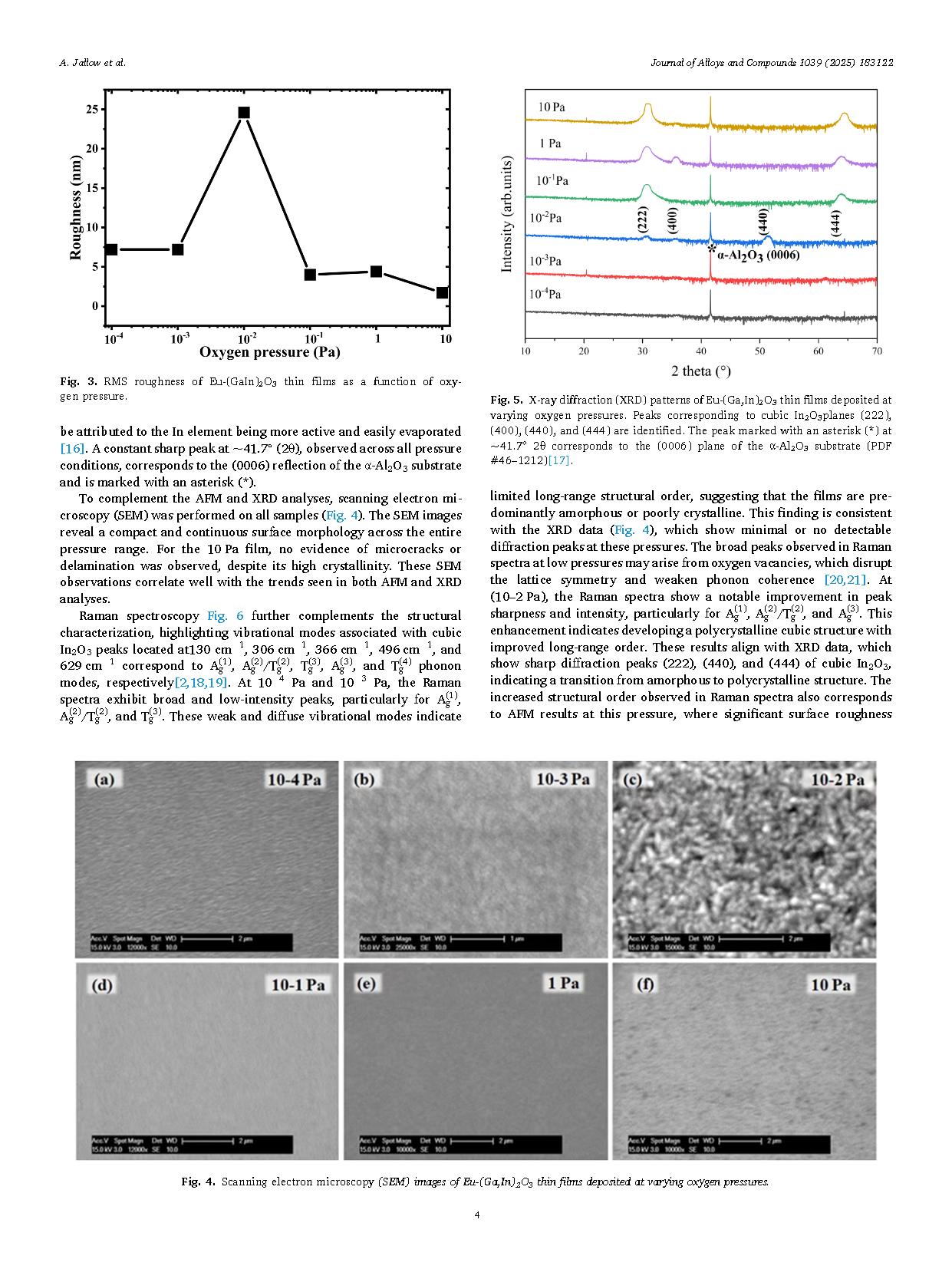
Fig. 1. X-ray diffraction (XRD) patterns of Eu-(Ga,In)2O3 thin films deposited at varying oxygen pressures. Peaks corresponding to cubic In2O3 planes (222), (400), (440), and (444) are identified. The peak marked with an asterisk (*) at ~41.7◦ 2θ corresponds to the (0006) plane of the α-Al2O3 substrate (PDF #46–1212)
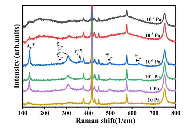
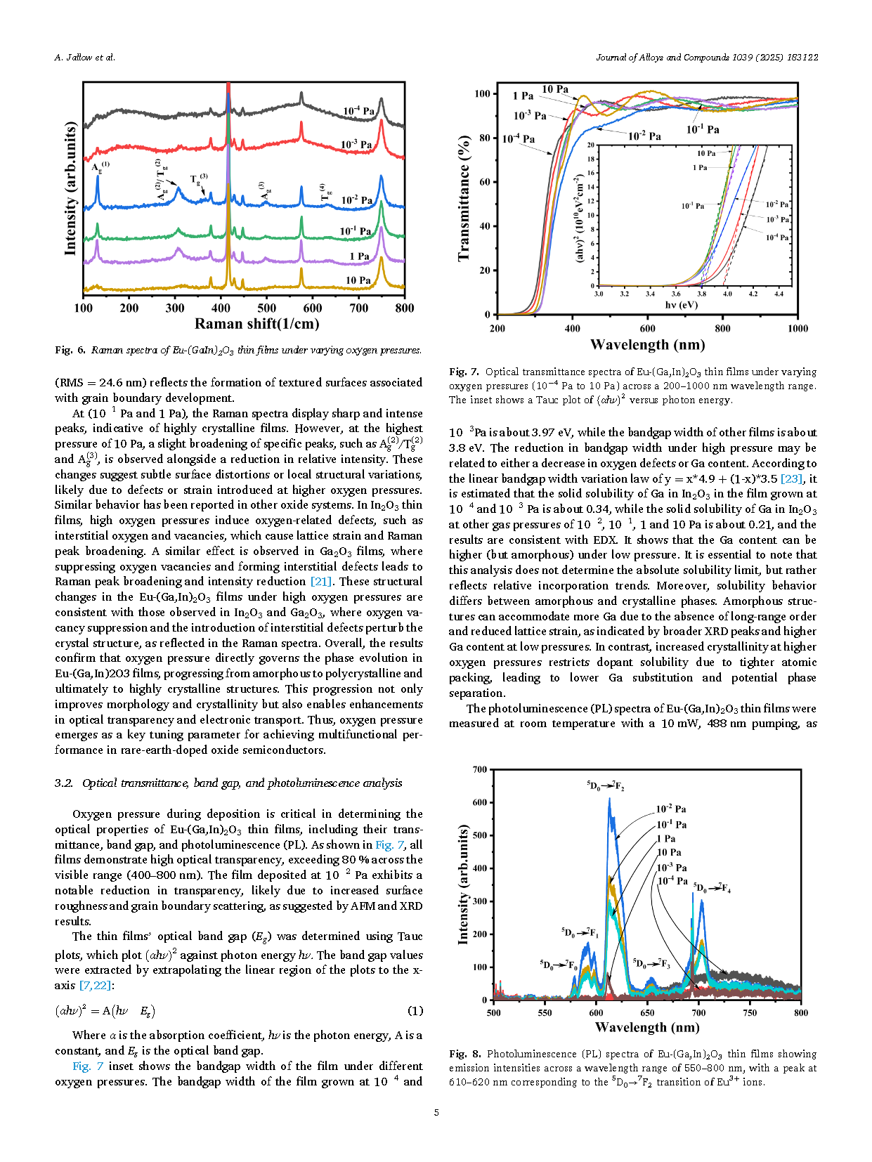
Fig. 2. Raman spectra of Eu-(GaIn)2O3 thin films under varying oxygen pressures.
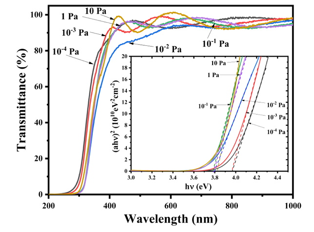
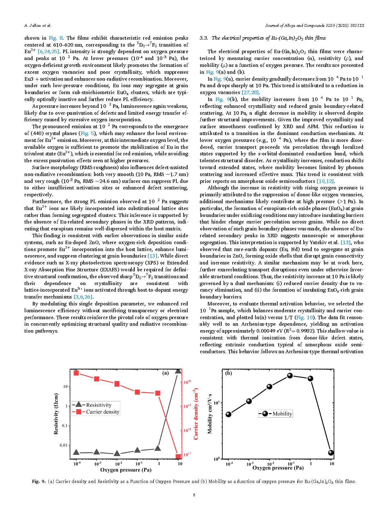
Fig. 3. Optical transmittance spectra of Eu-(Ga,In)2O3 thin films under varying oxygen pressures (10-4 Pa to 10 Pa) across a 200–1000nm wavelength range. The inset shows a Tauc plot of (αhν)2 versus photon energy.
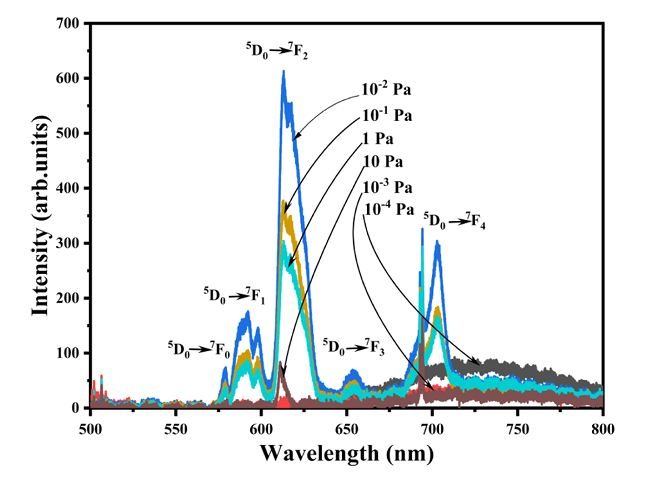
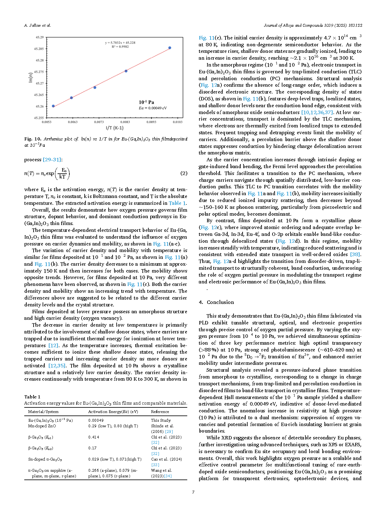
Fig. 4. Photoluminescence (PL) spectra of Eu-(Ga,In)2O3 thin films showing emission intensities across a wavelength range of 550–800nm, with a peak at 610–620nm corresponding to the 5D0→7F2 transition of Eu3+ ions.
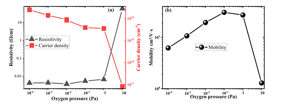
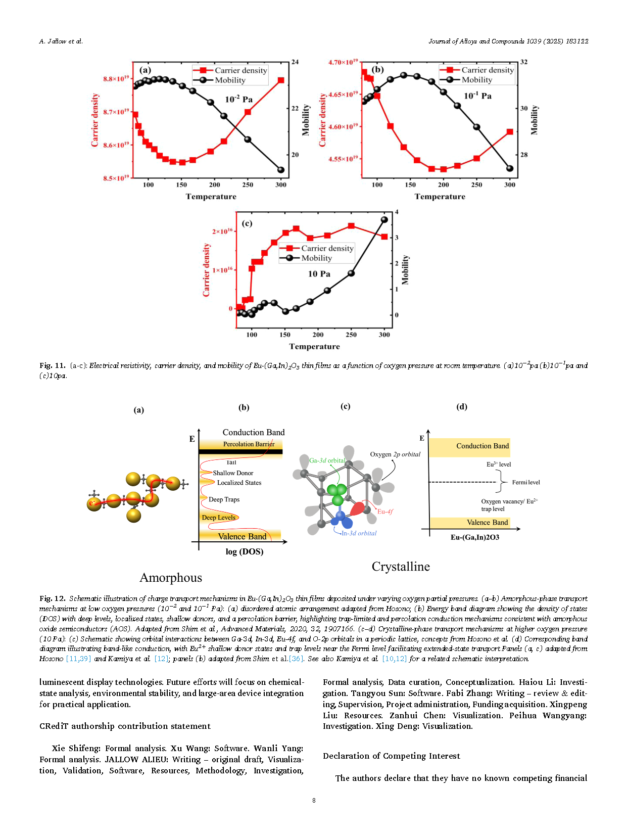
Fig. 5. (a) Carrier density and Resistivity as a Function of Oxygen Pressure and (b) Mobility as a function of oxygen pressure for Eu-(Ga,In)2O3 thin films.
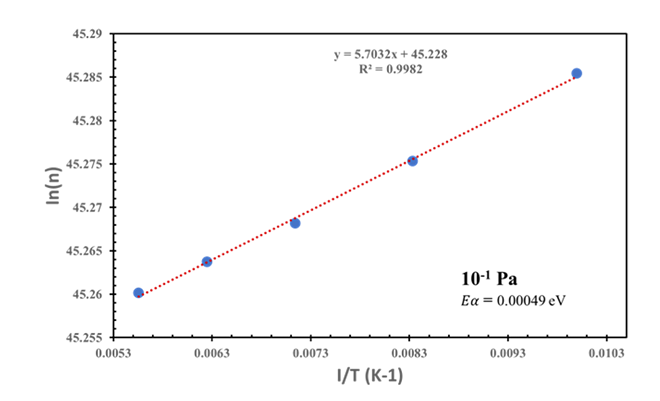
Fig. 6. Arrhenius plot of. ln(n) vs 1/T in for Eu-(Ga,In)2O3 thin filmdeposited at 10-1Pa.
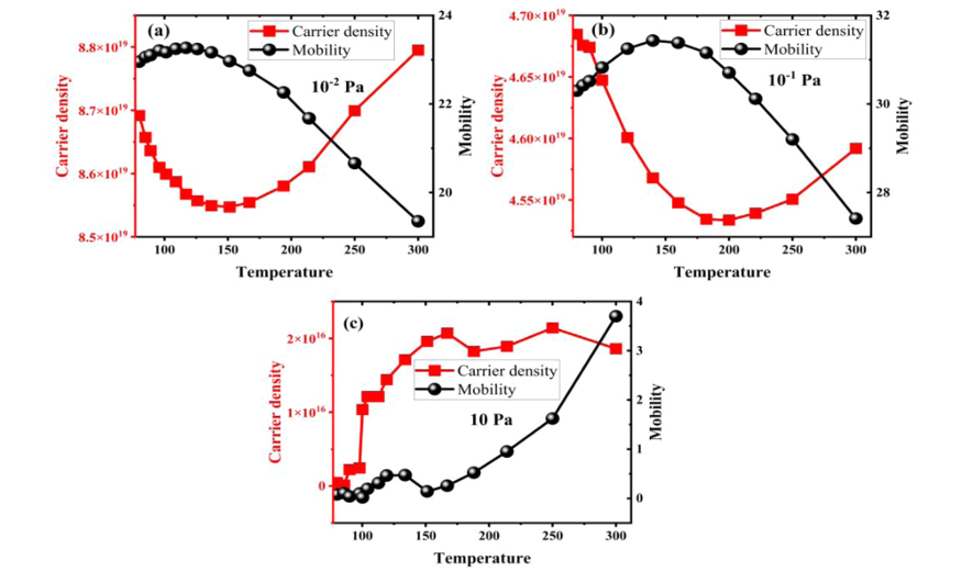
Fig. 7. (a-c): Electrical resistivity, carrier density, and mobility of Eu-(Ga,In)2O3 thin films as a function of oxygen pressure at room temperature. (a)10-2pa. (b)10-1 pa (c) 10 Pa.
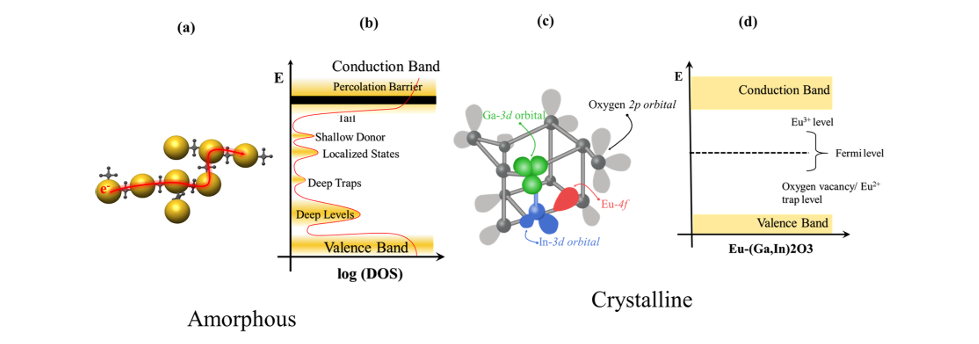
Fig. 8. Schematic illustration of charge transport mechanisms in Eu-(Ga,In)₂O₃ thin films deposited under varying oxygen partial pressures. (a–b) Amorphous-phase transport mechanisms at low oxygen pressures (10² and 10¹ Pa): (a) disordered atomic arrangement adapted from Hosono; (b) Energy band diagram showing the density of states (DOS) with deep levels, localized states, shallow donors, and a percolation barrier, highlighting trap-limited and percolation conduction mechanisms consistent with amorphous oxide semiconductors (AOS). (c–d) Crystalline-phase transport mechanisms at higher oxygen pressure (10 Pa): (c) Schematic showing orbital interactions between Ga-3d, In-3d, Eu-4f, and O-2p orbitals in a periodic lattice, concepts from Hosono et al. (d) Corresponding band diagram illustrating band-like conduction, with Eu²⁺ shallow donor states and trap levels near the Fermi level facilitating extended-state transport.
DOI:
doi.org/10.1016/j.jallcom.2025.183122