


Paper Sharing
【Domestic Papers】Tunable Superlinear Gallium Oxide Gate-All-Around Deep-Ultraviolet Phototransistor for Near-Field Imaging
日期:2025-09-10阅读:750
Prof. Long Shibing, Zhao Xiaolong, and Hou Xiaohu from the University of Science and Technology of China, together with their team, have published a paper titled “Tunable Superlinear Gallium Oxide Gate-All-Around Deep-Ultraviolet Phototransistor for Near-Field Imaging” in ACS Nano.
This work proposes a p–n heterojunction-based tunable superlinear Ga₂O₃ deep-ultraviolet (DUV) gate-all-around (GAA) phototransistor for near-field imaging. Leveraging the photo-gating effect, the device transitions from the cutoff state to the saturation conduction state as light intensity increases, exhibiting superlinear characteristics. Moreover, the light response can be flexibly switched between linear and superlinear modes via gate-voltage modulation. In addition, the device achieves an ultrafast response speed of 749 μs, attributed to the accelerated photocarrier recombination enabled by the GAA structure. The demonstrated superlinear photoresponse shows excellent focusing performance in near-field imaging, providing a feasible approach toward the development of superlinear photodetectors and their applications in near-field sensing systems.
Background
As the core front-end component of optoelectronic systems, photodetectors convert optical signals into electrical signals through the photoelectric effect of semiconductor materials, playing an irreplaceable role in fields such as automation control, high-precision imaging, and remote sensing. Traditional photodetectors rely on linear response mechanisms. However, with the rise of technologies such as the Internet of Things (IoT) and autonomous driving, conventional vision systems are facing challenges including high power consumption, high latency, and hardware redundancy. In recent years, photodetectors integrating both sensing and computing capabilities have emerged as a breakthrough approach. Among them, superlinear photoresponse detectors have attracted significant attention due to their unique capabilities—for example, selectively distinguishing and amplifying effective signals while suppressing surrounding diffracted light interference in near-field imaging.
The mechanisms for achieving superlinear photoresponse usually depend on microscopic interactions of specific materials, such as second harmonic generation processes or competitive mechanisms of dual recombination centers. However, these methods impose strict requirements on photosensitive materials, limiting the scalability of integrated device applications. By contrast, phototransistors—with their high gain, tunable operation, and strong compatibility for integration—show potential for material-independent superlinear detection.
Deep ultraviolet (DUV) detection technology offers significant advantages across multiple fields, and superlinear DUV detection is particularly critical for high-performance sensing and near-processing applications. Gallium oxide (Ga₂O₃), with its direct bandgap in the DUV spectrum, is regarded as an ideal material for DUV photodetectors. Nonetheless, its practical use is constrained by the difficulty of achieving effective p-type doping. On the other hand, nickel oxide (NiO), featuring high hole carrier concentration and mobility, can form high-quality heterojunctions with Ga₂O₃, combining Ga₂O₃’s DUV selectivity with NiO’s hole transport advantages.
Abstract
Superlinear photodetectors hold significant potential in intelligent optical detection systems, such as near-field imaging. However, their current realization imposes stringent requirements on photosensitive materials, thereby limiting the flexibility of the device integration for practical applications. Herein, a tunable superlinear Ga2O3 deep-ultraviolet gate-all-around (GAA) phototransistor based on a p–n heterojunction has been proposed. Benefiting from the photogating effect, the device transitions from a cutoff to a saturated conducting state with increasing light intensity, exhibiting superlinear characteristics. This behavior can be electrically modulated via gate voltage, enabling flexible switching between linear and superlinear photoresponse. Additionally, it demonstrates an ultrafast response speed (749 μs), attributed to the junction-based GAA structure that accelerates the recombination of photogenerated carriers. Finally, the superlinear photoresponse of the Ga2O3 GAA transistor has been applied to near-field imaging, achieving nice focusing effects on images. Our research provides a feasible approach for the realization of superlinear photodetectors and their application in near-field sensing systems.
Experimental Process
The researchers first carried out ultrasonic cleaning on the SiO₂ substrate and the Ga₂O₃ substrate, followed by the fabrication of NiO thin films via photolithography and magnetron sputtering. Ga₂O₃ nanosheets were mechanically exfoliated using Scotch tape and subsequently transferred onto PDMS, where they were precisely aligned with the central NiO region. Through multiple rounds of photolithography and electron-beam evaporation, Ti/Au source/drain electrodes and Ni/Au gate electrodes were fabricated.
Highlights
1、A tunable superlinear Ga₂O₃ deep-ultraviolet gate-all-around (GAA) phototransistor based on a p–n heterojunction is proposed, enabling the switching of photoresponse from linear to superlinear under different light intensities.
2、Voltage modulation is employed to dynamically tune the superlinear exponent, offering greater flexibility for photodetector applications.
3、The application of superlinear photoresponse in near-field imaging is demonstrated, achieving favorable focusing effects through software simulation and providing a new technical strategy for high-precision imaging.
4、The device exhibits an ultrafast response speed (749 μs), attributed to the GAA structure that accelerates the recombination of photogenerated carriers, making it potentially advantageous for fast imaging and real-time sensing applications.
Conclusion
In this study, a Ga₂O₃ phototransistor with a gate-all-around (GAA) structure was proposed, based on a high-quality NiO/Ga₂O₃ p–n junction and a precise fixed-position transfer technique of Ga₂O₃ nanosheets. The device demonstrates strong channel controllability, exhibiting low leakage characteristics and fast response capability. Through the photo-gating effect, a transition from the OFF state to the saturation state was achieved, thereby realizing a superlinear photoresponse (α = 5.54). Benefiting from the high-quality heterojunction and the GAA transistor structure that accelerates the recombination of photogenerated carriers, the device exhibited an ultrafast response speed (749 μs). Leveraging this superlinear photoresponse, near-field imaging focusing was successfully demonstrated through software simulations. This work provides a feasible approach for developing compact and high-speed photodetectors for imaging systems, where the synergistic enhancement of the photoelectric effect and transistor architecture highlights significant potential for optical sensing applications.
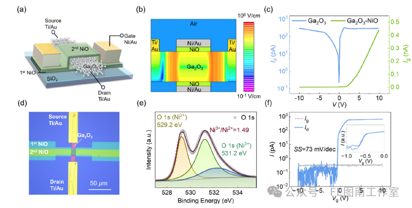
Figure 1. Design and electrical characteristics of the junction-type GAA phototransistor based on the p-NiO/n-Ga₂O₃/p-NiO structure. (a) Schematic illustration of the device with a p–n–p sandwich structure. (b) Simulated electric field distribution of the junction-type GAA device under reverse-biased p–n junction conditions. (c) I–V characteristics of the Ga₂O₃ nanosheet terminals and the p-NiO/n-Ga₂O₃ junction under dark conditions. (d) Optical microscope image of the device. (e) XPS fine spectrum of the NiO 1s peak and corresponding peak deconvolution. (f) Three-terminal double-sweep transfer characteristics and leakage current curve of the device. The inset shows the magnified transfer curve.
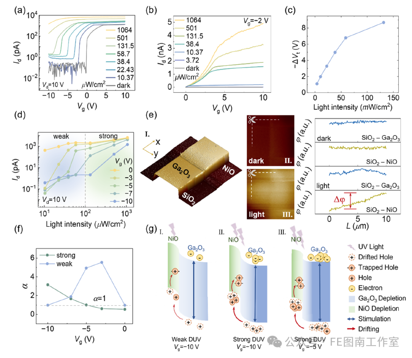
Figure 2. Optoelectronic characteristics and mechanism of the Ga₂O₃ GAA phototransistor. (a) Transfer characteristics of the device under varying light intensities. (b) Output curves of the device under deep-ultraviolet illumination. (c) Dependence of threshold voltage shift (ΔVt) on light intensity. (d) Photocurrent variation with light intensity and segmented fitting regions. (e) KPFM results of the p-NiO/n-Ga₂O₃/p-NiO sandwich structure: I. scan area and material schematic; II. surface potential distribution in the dark; III. surface potential distribution under illumination. The extracted potential variation along the dashed line is shown on the right. (f) Variation of the segmented fitting parameter α with gate bias. (g) Schematic of energy band diagrams and carrier transport under combined photovoltaic and photoconductive effects: I. weak light at moderate gate bias; II. medium light at moderate gate bias; III. strong light at moderate gate bias; IV. medium light at negative gate bias; V. medium light at positive gate bias.
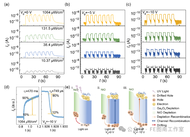
Figure 3. Transient characteristics and mechanism interpretation of the junction-type GAA phototransistor. (a) Transient response of the device under different light intensities at Vg = 0 V, (b) Vg = –5 V, and (c) Vg = –10 V. (d) Mechanism analysis of the response speed differences. (e) Energy band diagrams and carrier dynamics: I. original state; II. under UV illumination; III. after light-off at Vg = 0 V; IV. after light-off at Vg = –10 V. By modulating the two recombination processes, the device response speed can be controlled via gate voltage.
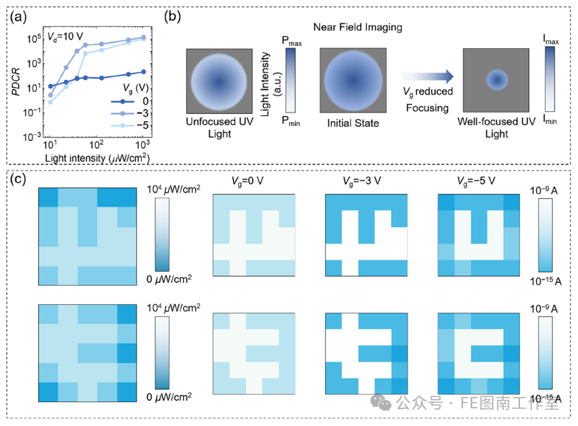
Figure 4. Near-field imaging simulation based on the GAA phototransistor. (a) Superlinear characteristics under different gate voltages. (b) Application to near-field imaging. (c) Simulated imaging results of the device at different gate voltages. By tuning Vg, the near-field imaging becomes progressively clearer.
https://doi.org/10.1021/acsnano.5c06915
